
Integrated microphone

Active Publication Date: 2010-09-14
INVENSENSE
View PDF81 Cites 116 Cited by
  • Summary
  • Abstract
  • Description
  • Claims
  • Application Information

AI Technical Summary

Benefits of technology

The patent describes a method and apparatus for making a microphone with a variable capacitance. The method involves depositing high temperature material on a die to form the structure that contributes to the variable capacitance, and then forming circuitry on the die to detect the variable capacitance. A released diaphragm or unreleased structure can be formed from the deposition material. The method also involves adding sacrificial material between the deposition material and the die, and selectively removing portions of the deposition material and sacrificial material to suspend the deposition material. The microphone can be formed on a SOI wafer or a single layer silicon wafer. The technical effects of the invention include improved sensitivity and accuracy of detecting the variable capacitance, and improved performance of the microphone in high-temperature environments.

Problems solved by technology

Forming such circuitry on the same die as the microphone, however, generally presents a number of challenges.

Method used


Image

  • Integrated microphone
  • Integrated microphone
  • Integrated microphone

Examples


Embodiment Construction

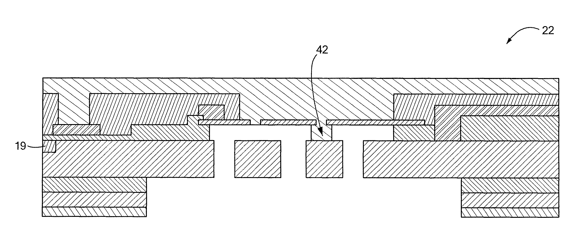
[0022]In illustrative embodiments, a MEMS microphone has both structure and circuitry supported and / or formed at least in part by a silicon-on-insulator wafer (“SOI wafer”). In other embodiments, a method of forming a MEMS microphone deposits high temperature deposition material on a die before adding circuitry to the same die. Other embodiments, however, deposit low temperature deposition material on the die after forming circuitry on the same die. Details of illustrative embodiments are discussed below.

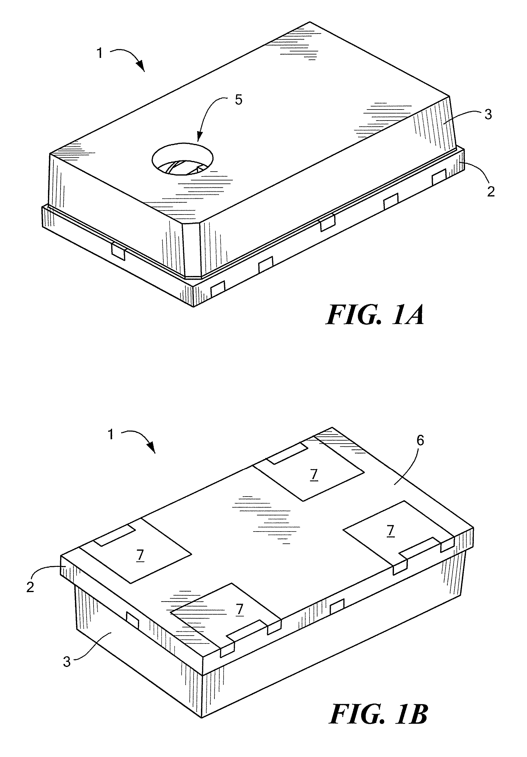
[0023]FIG. 1A schematically shows a top, perspective view of a packaged microphone 1 that may be configured in accordance with illustrative embodiments of the invention. In a corresponding manner, FIG. 1B schematically shows a bottom, perspective view of the same packaged microphone 1.

[0024]The microphone 1 shown in those figures has a package base 2 that, together with a corresponding lid 3, forms an interior chamber containing a MEMS microphone chip 10 (discussed below, see FIGS. ...


PUM


Abstract

A method of forming a microphone having a variable capacitance first deposits high temperature deposition material on a die. The high temperature material ultimately forms structure that contributes to the variable capacitance. The method then forms circuitry on the die after depositing the deposition material. The circuitry is configured to detect the variable capacitance.

Description

PRIORITY[0001]This patent application claims priority from provisional U.S. patent application Ser. No. 60 / 757,703, filed Jan. 9, 2006, entitled, “INTEGRATED MICROPHONE,” and naming John R. Martin, Jason W. Weigold, and Timothy J. Brosnihan as inventors, the disclosure of which is incorporated herein, in its entirety, by reference.[0002]This patent application also is a continuation-in-part of U.S. patent application Ser. No. 11 / 044,612, filed Jan. 27, 2005, assigned publication number US2005 / 0255677, entitled, “INTEGRATED CIRCUIT WITH IMPURITY BARRIER,” and naming Jason W. Weigold, Thomas D. Chen, Denis Mel O'Kane, Clair N. Leveugle, Stephen Alan Brown, and William A. Nevin as inventors, the disclosure of which is incorporated herein, in its entirety, by reference.FIELD OF THE INVENTION[0003]The invention generally relates to microphones and, more particularly, the invention relates to microphones and methods of producing microphones having both structure and circuitry.BACKGROUND O...

Claims


Application Information

Patent Timeline
Patent Type & Authority Patents(United States)
IPC IPC(8): H01L29/84H04R25/00
CPCB81C1/00246H04R1/04H04R19/005H04R31/006B81B2201/0257B81C2203/0728H04R19/04
Inventor WEIGOLD, JASON W.MARTIN, JOHN R.BROSNIHAN, TIMOTHY J.
Owner INVENSENSE
Learn More