Power ranging transmit RF power amplifier

Active Publication Date: 2010-09-14
PSEMI CORP
View PDF11 Cites 56 Cited by
  • Summary
  • Abstract
  • Description
  • Claims
  • Application Information

AI Technical Summary

Benefits of technology

[0009]One aspect of the present teachings is an RF PA that amplifies an RF signal in a selectable plurality of output power ranges and comprises a plurality of distinct active amplifier circuit devices. The RF PA is fabricated such that during operation in a high power range, a lower power active amplifier device amplifies the signal first, while a distinct high power active amplifier circuit device subsequently provides final amplification of the signal, but during operation in a lower power range, the lower power active amplifier circuit device provides the final signal amplification. The RF PA may be further defined by requiring any combination of the following additional features insofar as they are functionally compatible. The additional features may include the following: the RF PA may be required to be fabricated entirely on a single contiguous integrated circuit die; and/or the RF PA may be required to comprise only active devices that are fabricated by a common set of semiconductor processing techniques associated with a particular type of semiconductor wafer; and/or the RF PA may comprise a single type of semiconductor wafer, or it may be entirely integrated on a single semiconductor wafer; and/or the RF PA may required to have no active, switchable path in series with the signal subsequent to the high power active amplifier circuit; and/or the RF PA may be required to actively switch impedance matching elements between the high and lower power modes, in which case the RF PA may be further required to incorporate all such switched impedance matching elements as part of the same semiconductor die(s) incorporating the active amplifier circuit devices, and/or it may be further required to incorporate all active devices that switch the impedance matching elements on the same semiconductor die(s); and/or the RF PA may be required to amplify the signal by each of the plurality of active amplifier circuit devices in a high power mode, while in the lower power mode quiescent (bias) current in the high power active amplifier circuit device is substantially disabled, which may mean that its quiescent current is reduced to a value that is less than 5%, or less than 2%, or less than 1%, or even less than 0.5% of its quiescent current when operating in the high power mode; and/or the RF PA may be required to have a multiplicity of distinct amplifier circuit devices that all amplify the signal in the high power mode; and/or all active devices of the RF PA may be required to be FETs having an insulated gate; and/or the RF PA may be required to consist of only one, or alternatively of at least one, semiconductor die having a fully insulating substrate; and/or the RF PA may be required to be implemented in silicon on insulator (SOI) semiconductor material; and/or the RF PA may be required to comprise of a solitary, or alternatively of at least one, silicon on sapphire semiconductor die; and/or the RF PA may be required to incorporate mode and bias

Problems solved by technology

Designs that increase signal quality and transmit power will generally increase operational range, but will thereby negatively affect battery life and/or cost unless the PA power efficiency is also increased.
However, a PA design that is highly efficient at a selected first powe

Method used


Image

  • Power ranging transmit RF power amplifier
  • Power ranging transmit RF power amplifier
  • Power ranging transmit RF power amplifier

Examples


Embodiment Construction

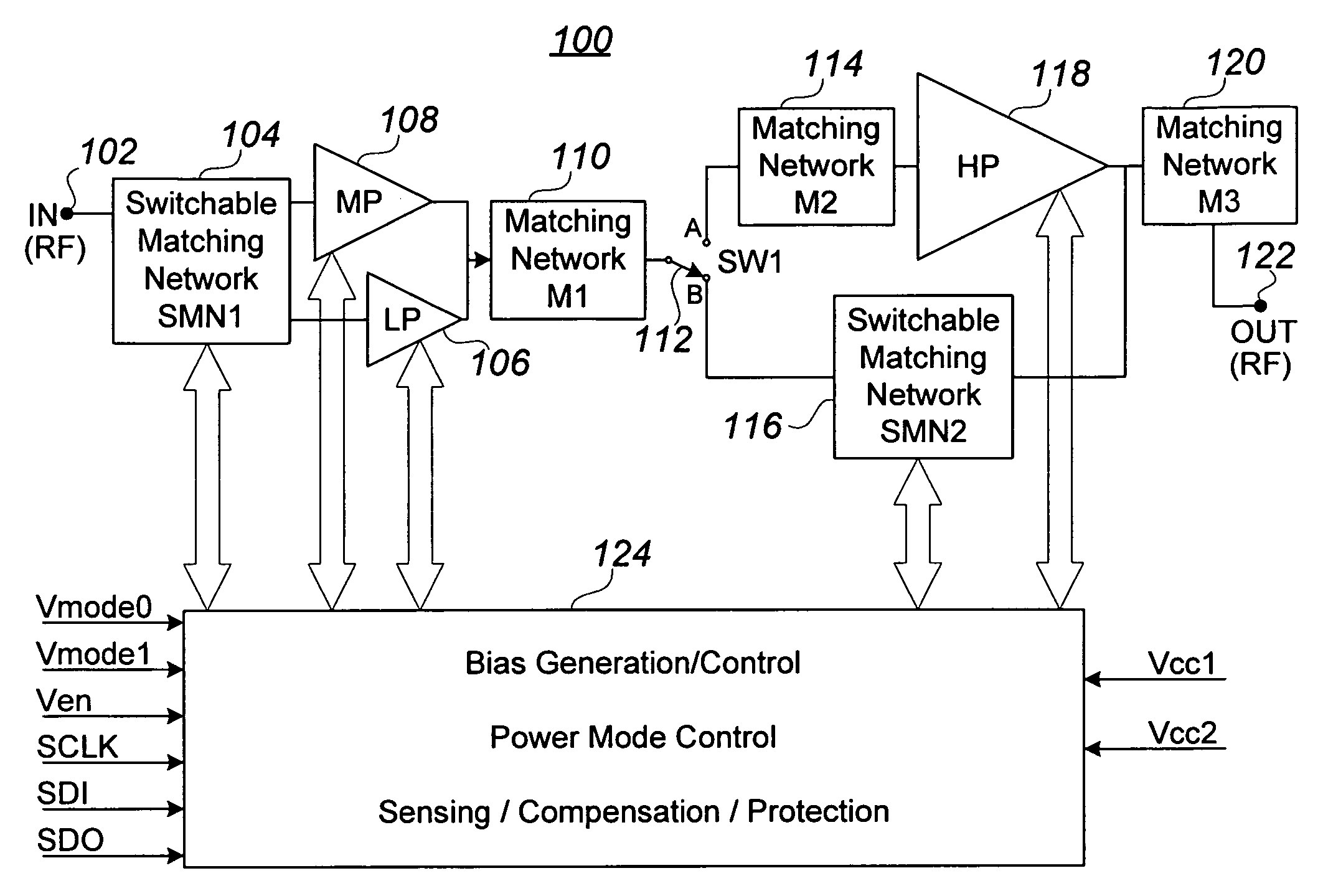
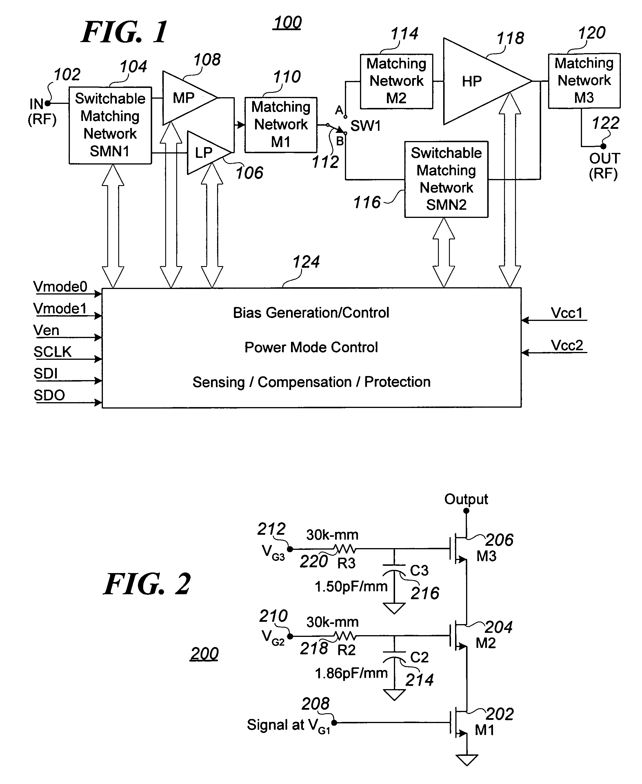
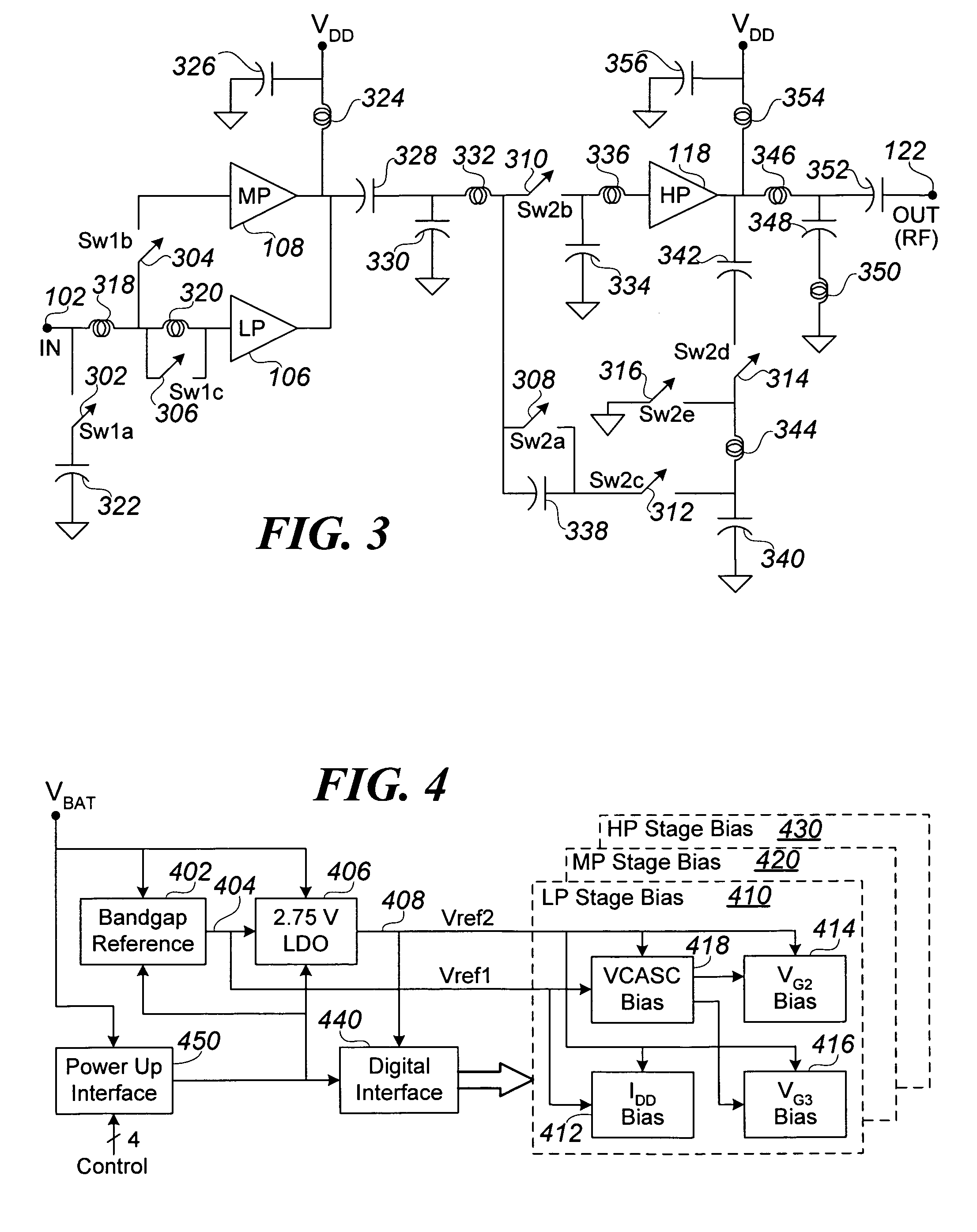
[0016]Embodiments of RF PAs (Radio Frequency Power Amplifiers) as described herein may generally be fabricated using any number of alternative semiconductor materials and manufacturing processes, as will be appreciated by those who are knowledgeable and experienced in respect of such alternative semiconductors and processes. However, the preferred embodiments have been developed in accordance with an Ultra Thin Silicon on Insulator semiconductor, and corresponding processing steps, because that is the semiconductor type with which the inventors presently work most often. Only reasonable experimentation will be required to adapt the structures and methods described herein for such alternative semiconductor types and processes. Hence, such alternative embodiments are fairly taught by the description set forth below, and are encompassed by any statement or claim that defines the invention without explicitly excluding or rendering such alternative embodiments incompatible. Details of th...


PUM


Abstract

An RF PA operable in two or more selectable power ranges is disclosed. Switches configure the circuit for each range such that an amplifier device corresponding to the range provides final amplification, and all lower power amplifier devices also amplify the signal. An exemplary design includes a low power amplifier configurable for operation solo, or in parallel with a medium power amplifier, to deliver an appropriately matched signal either directly to the RF PA output, or first to the input of a high power amplifier for the highest power range. The signal in all ranges of the exemplary design is conditioned in part by the matching circuitry disposed between the high power amplifier and the RF PA output, which traverses no switches in high power range operation. The entire RF PA, including switches, control and matching circuitry, is fabricated on a single monolithic integrated circuit, an achievement may be facilitated by UTSI CMOS processing.

Description

[0001]This application claims priority under 35 USC 119 to U.S. Provisional Application 61 / 010,824 filed Jan. 12, 2008 and entitled “Power Ranging Transmit Power Amplifier,” the entire contents of which are hereby incorporated herein by reference.BACKGROUND[0002]1. Field[0003]The present disclosure relates to electronic integrated circuits (“ICs”), and more specifically to RF power amplifier (“PA”) integrated circuits.[0004]2. Related Art[0005]Most radio transceivers, such as the cell phones that are a ubiquitous feature of modern life, require an RF PA circuit to boost the transmit signal to a level sufficient to be received by a target transceiver, such as a cellular base station. In this highly competitive field, consumers value increases in transceiver features such as battery life, operational range and signal quality. The RF power amplifier strongly impacts each of these features. Designs that increase signal quality and transmit power will generally increase operational range...

Claims


Application Information

Patent Timeline
IPC IPC(8): H03F3/68
CPCH03F1/223H03F1/56H03F3/195H03F3/72H03F2203/7233
Inventor LI, YANGBROUGHTON, ROBERTBONKOWSKI, JAMESBACON, PETER
Owner PSEMI CORP
Why Eureka
Try Eureka