Neutral beam-assisted atomic layer chemical vapor deposition apparatus and method of processing substrate using the same

a technology atomic layer, which is applied in the direction of chemical vapor deposition coating, electric discharge tubes, coatings, etc., can solve the problems of requiring a gap-fill process in sub-65 nm class devices, hdpcvd apparatus is expensive, and the gap-fill process is not easy to achiev

Inactive Publication Date: 2010-09-21
RES & BUSINESS FOUND SUNGKYUNKWAN UNIV
View PDF3 Cites 284 Cited by
  • Summary
  • Abstract
  • Description
  • Claims
  • Application Information

AI Technical Summary

Problems solved by technology

However, this process has a difficulty in that, after the trench pattern is formed, a gap-fill process of filling the trench pattern with an oxide layer acts as a bottleneck.
In contrast, in the case of 65 nm class devices, the gap-fill process using the HDPCVD apparatus encounters a limitation.
These apparatuses are also expensive, and thus have a difficulty in profile control, so that they have a problem in that a process capable of performing the gap-fill process in sub-65 nm class devices is required.

Method used


Image

  • Neutral beam-assisted atomic layer chemical vapor deposition apparatus and method of processing substrate using the same
  • Neutral beam-assisted atomic layer chemical vapor deposition apparatus and method of processing substrate using the same
  • Neutral beam-assisted atomic layer chemical vapor deposition apparatus and method of processing substrate using the same

Examples


Embodiment Construction

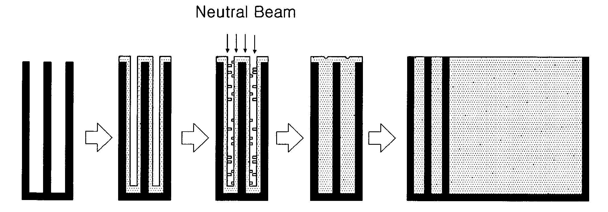
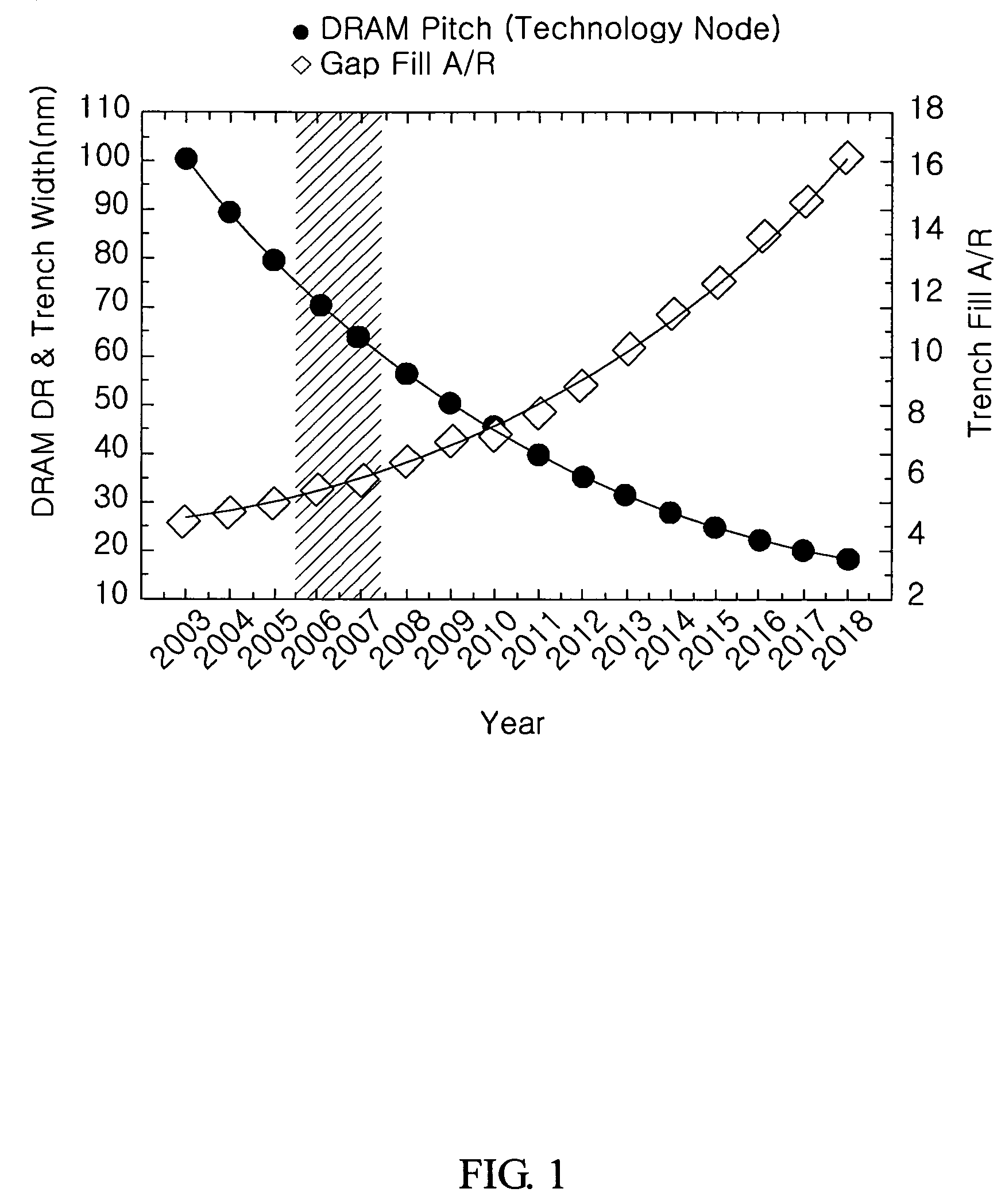
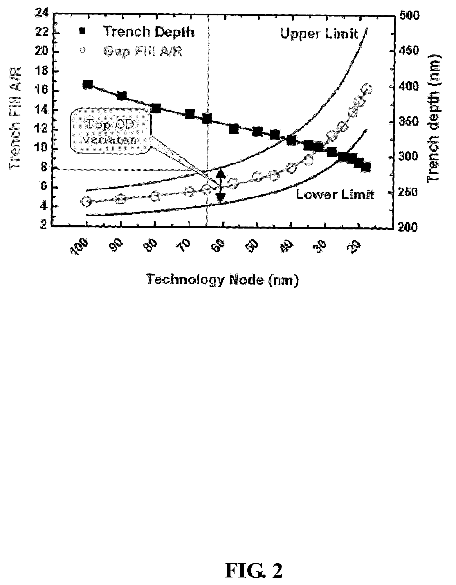
[0038]The present invention may increase low oxide-layer uniformity, which is caused by formation of a seam or void, by applying neutral beams to an oxide layer using a neutral beam generator of an atomic layer chemical vapor deposition (ALCVD) apparatus while depositing the oxide layer in order to form a trench pattern in a semiconductor device, and fill a spacing between cells at high density while reducing the spacing.

[0039]Hereinafter, the present invention will be explained in detail with reference to the accompanying drawings.

[0040]First, the configuration of a neutral beam-assisted ALCVD apparatus according to the present invention will be described with reference to the accompanying drawings.

[0041]FIG. 3 is a schematic perspective view of a neutral beam-assisted ALCVD apparatus according to the present invention, and FIG. 4 is a schematic perspective view of a neutral beam generator in the neutral beam-assisted ALCVD apparatus illustrated in FIG. 3.

[0042]As illustrated, the ...


PUM

PropertyMeasurementUnit
widthaaaaaaaaaa
incident angleaaaaaaaaaa
widthaaaaaaaaaa

Abstract

A neutral beam-assisted atomic layer chemical vapor deposition (ALCVD) apparatus is provided for uniformly depositing an oxide layer filling a planarization layer or a trench to increase uniformity and density of the oxide layer using neutral beams generated by a neutral beam generator without a seam or void occurring in an atomic layer deposition (ALD) or ALD-like chemical vapor deposition (CVD) process, thereby solving problems on the void or seam and low density occurring when a high-density planarization layer or a shallow trench having a width of 65 nm or less is formed, and improving a next generation oxide layer isolation process. The neutral beam-assisted ALCVD apparatus includes: an ALCVD apparatus, which deposits an oxide layer in order to form a pattern in a semiconductor substrate; and a neutral beam generator, which converts ion beams to neutral beams in order to remove a seam or void in the oxide layer deposited between the patterns, and applies the neutral beams to the oxide layer deposited to form the pattern.

Description

CROSS-REFERENCE TO RELATED APPLICATION[0001]This application claims the benefit of Korean Patent Application No. 2008-0012330, filed Feb. 11, 2008, the disclosure of which is hereby incorporated herein by reference in its entirety.BACKGROUND OF THE INVENTION[0002]1. Field of the Invention[0003]The present invention relates to a neutral beam-assisted atomic layer chemical vapor deposition (ALCVD) apparatus, and more particularly, to a neutral beam-assisted atomic layer chemical vapor deposition (ALCVD) apparatus and a method of processing a substrate using the same, capable of improving density of a planarization layer and preventing non-uniform deposition in the process of filling a gap or a shallow trench with an oxide layer by adding a neutral beam processing process.[0004]2. Description of the Related Art[0005]In general, chemical vapor deposition (CVD) is one of the industrial methods of forming a thin layer of, for instance, silicon on a substrate in the process of fabricating,...

Claims


Application Information

Patent Timeline
Patent Type & Authority Patents(United States)
IPC IPC(8): H01L21/31H01L21/469
CPCC23C16/44C23C16/45536H01L21/3141H01L21/31604H01J2237/0041H01J2237/08H01J2237/3142H01L21/0228C23C16/455C23C16/00
Inventor YEOM, GEUN-YOUNGPARK, BYOUNG-JAEKIM, SUNG-WOOLIM, JONG-TAE
Owner RES & BUSINESS FOUND SUNGKYUNKWAN UNIV
Why Eureka
Try Eureka