

Microelectronic multiple electron beam emitting device
a technology of electron beam and emitting device, which is applied in the field of microelectronic multiple electron beam emitting device, can solve the problems of bringing the limit domain of usable wavelength of these photolithography processes closer to the limit domain, and it is difficult to further reduce the minimum measurement or critical dimension of patterns
- Summary
- Abstract
- Description
- Claims
- Application Information
AI Technical Summary
Benefits of technology
Problems solved by technology
Method used
Image

Examples
Embodiment Construction
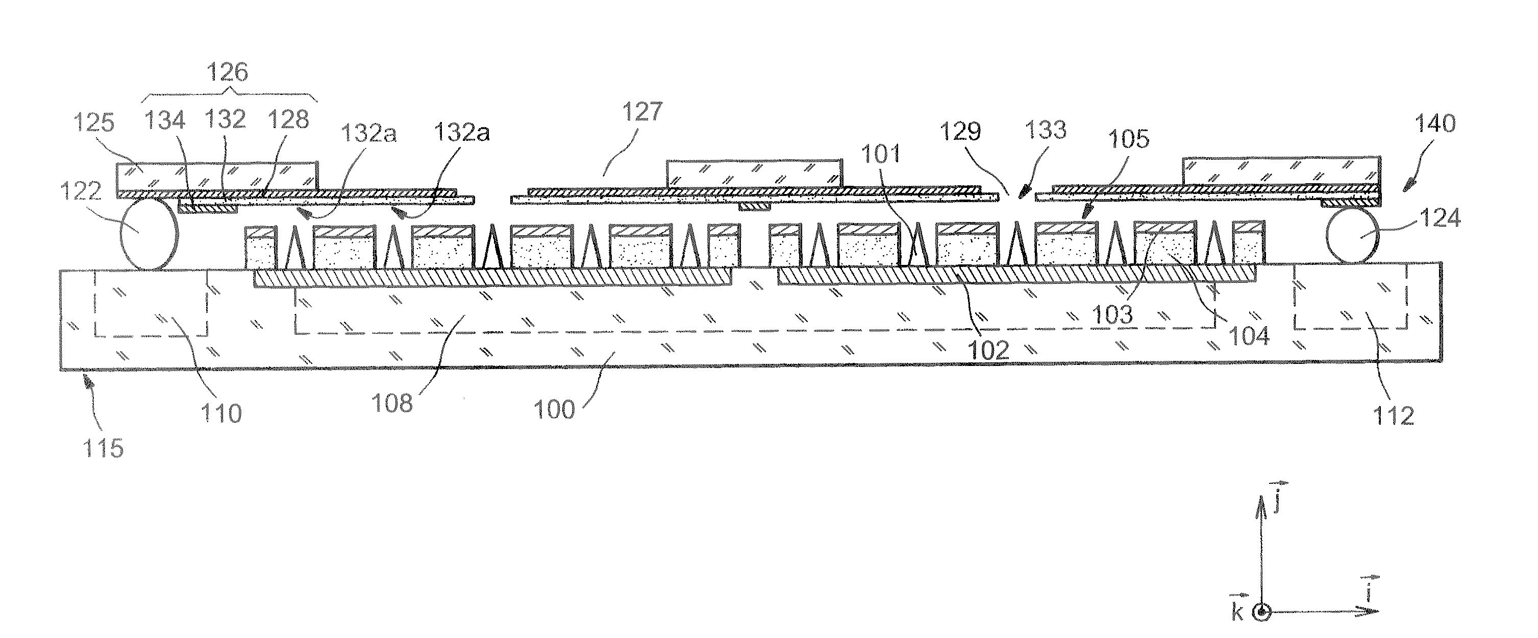
[0013]The present invention makes it possible in particular to reduce the phenomena of temporal and spatial instability of beams of electrons and lack of uniformity between said beams in “multi-beam” electron emitter devices.
[0014]The invention concerns an electron emitter device, in particular microelectronic and / or formed in thin films, and capable of emitting several beams of electrons, comprising:[0015]first means comprising at least one first substrate and a plurality N1 (where N1 is a integer greater than 1) of sources or micro-sources of electrons formed on a first substrate,[0016]second means capable of collecting electrons from said micro-sources and emitting other electrons following this collection, said second means comprising at least one layer known as “collection layer” located opposite the micro-sources and in which is formed a plurality of secondary electron emitters, for example a plurality or a number N2 (N2>1) of openings.
[0017]The number N2 of openings may be di...
PUM
 Abstract
Description
Claims
Application Information