Data preparation for multiple mask printing

a technology of data preparation and mask printing, applied in the field of photolithographic processing, can solve the problems of inability of photolithographic printing system to print features on wafers, and the lack of masks contained on them

Active Publication Date: 2010-09-21
SIEMENS PROD LIFECYCLE MANAGEMENT SOFTWARE INC
View PDF117 Cites 14 Cited by
  • Summary
  • Abstract
  • Description
  • Claims
  • Application Information

AI Technical Summary

Problems solved by technology

As the circuit elements become smaller and smaller, the ability of a photolithographic printing system to print the features on the wafer becomes increasingly diminished.
Optical and other process distortions occur such that the pattern contained on the mask will often not match the pattern of circuit elements that is printed on the wafer.

Method used


Image

  • Data preparation for multiple mask printing
  • Data preparation for multiple mask printing
  • Data preparation for multiple mask printing

Examples


Embodiment Construction

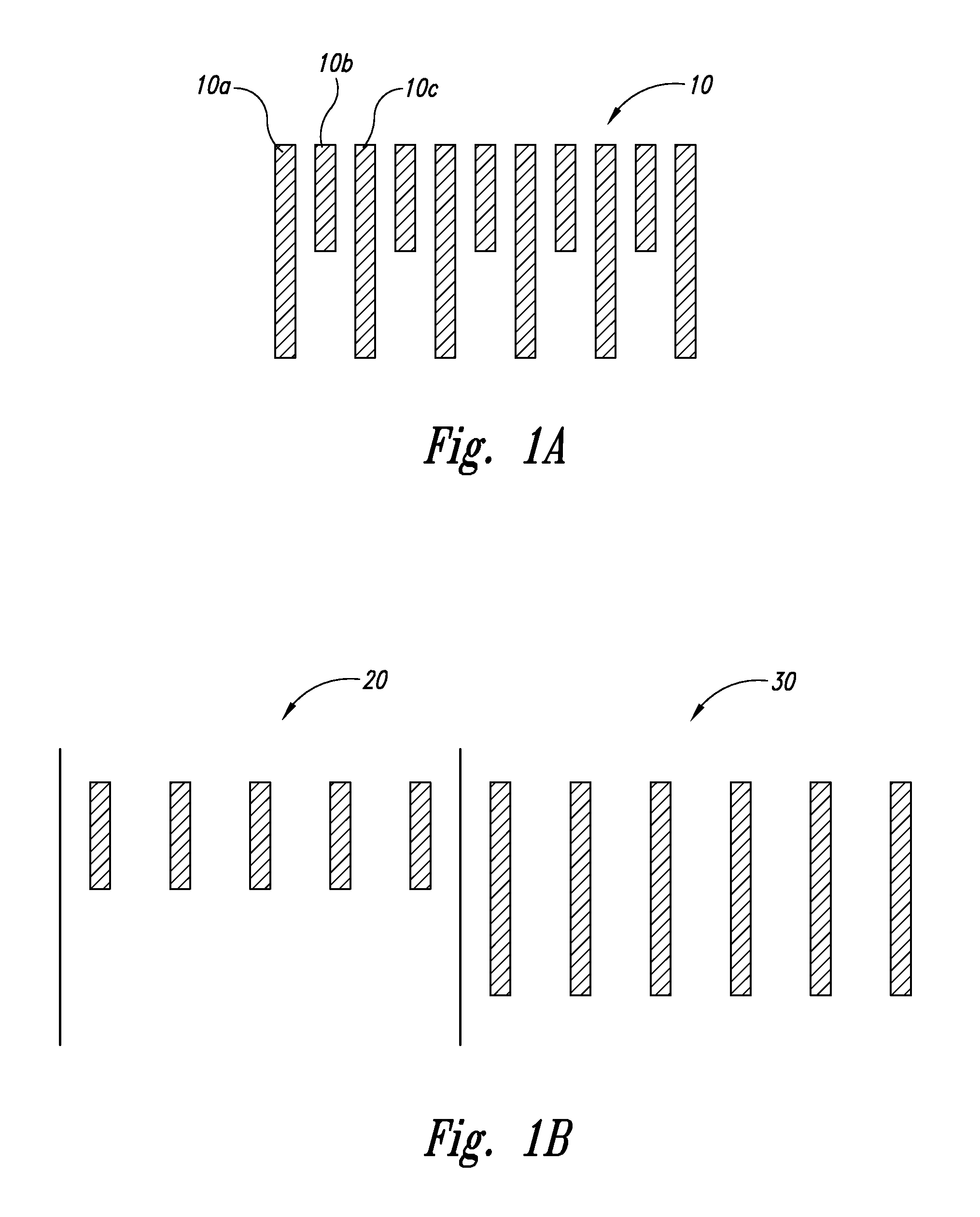
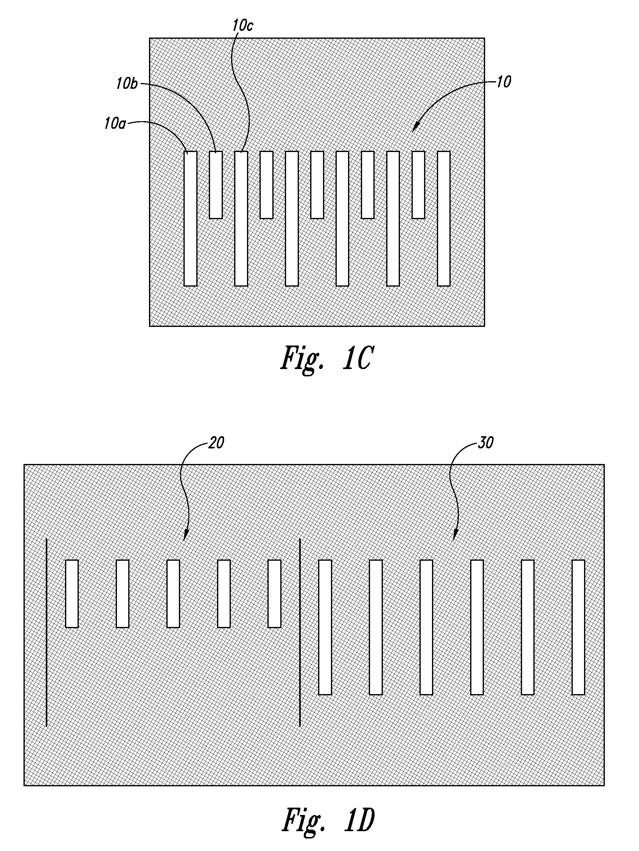
[0018]FIGS. 1A and 1B illustrate the basic operation of a double patterning photolithographic printing process. A target layout 10 includes a number of features 10a, 10b, 10c, etc., that are to be printed on a semiconductor wafer. The minimum pitch or distance between each feature that can be imaged on a wafer is determined by the resolving ability of the photolithographic printing system. One technique used to print features that are closer together than the photolithographic printing system would normally allow is a double patterning technique.

[0019]With double patterning, the desired pattern of features to be printed on a wafer is divided among two or more masks wherein each mask prints one set of features on the wafer. The masks print sets of features that are interleaved such that the features printed by both masks have a pitch that is closer than that obtainable with a single mask alone. For example, as shown in FIG. 1B, the desired target pattern 10 is divided into a first se...


PUM


Abstract

A method for preparing data to create two or more masks required to print a desired feature pattern with a multiple mask technique. In one embodiment of the invention, a target feature pattern is separated into two or more groups or data layers with a coloring algorithm. Coloring conflicts or adjacent features that are within a predetermined distance of each other and are assigned to the same group or data layer are identified. Cutting boxes are added to a feature to divide a feature into two or more smaller features. A coloring algorithm is re-applied to the layout including the cutting boxes to assign the features into different groups or data layers. Data in each group or data layer is used to define a mask to print the target feature pattern.

Description

FIELD OF THE INVENTION[0001]The present invention relates to photolithographic processing, and in particular to mask data preparation techniques for lithographic processes using multiple mask photolithography.BACKGROUND OF THE INVENTION[0002]Most integrated circuits are created by exposing a pattern of features contained on a mask (sometimes referred to as a reticle) onto a silicon wafer that is coated with photosensitive materials. The exposed wafer is then chemically and mechanically processed to create corresponding objects or circuit elements on the wafer. Other circuit patterns are then exposed onto the wafer to build up the integrated circuit layer by layer.[0003]As the circuit elements become smaller and smaller, the ability of a photolithographic printing system to print the features on the wafer becomes increasingly diminished. Optical and other process distortions occur such that the pattern contained on the mask will often not match the pattern of circuit elements that is...

Claims


Application Information

Patent Timeline
Patent Type & Authority Patents(United States)
IPC IPC(8): G06F17/50
CPCG03F1/144G03F1/68G03F1/70
Inventor PARK, JEA-WOOSAHOURIA, EMILE Y.
Owner SIEMENS PROD LIFECYCLE MANAGEMENT SOFTWARE INC
Why Eureka
Try Eureka