Method for forming side wirings

a technology of side wirings and wires, applied in the direction of electrical equipment, semiconductor devices, semiconductor/solid-state device details, etc., can solve the problem that the conductive paste cannot be continuously spit out according to its viscosity, and achieve the effect of high density and large capacity

Inactive Publication Date: 2010-10-05
SHINKO ELECTRIC IND CO LTD
View PDF3 Cites 0 Cited by
  • Summary
  • Abstract
  • Description
  • Claims
  • Application Information

AI Technical Summary

Benefits of technology

[0018]The wettability between the wiring and the conductive paste is satisfactory. For this reason, when the wiring extended out to the side surface of the semiconductor element is brought into contact with the conductive paste, the conductive paste is likely to be collected on the periphery of the wiring so that contact of the pertinent side wiring with an adjacent side wiring can be avoided. Thus, reliability of the semiconductor apparatus finally produced can be improved.
[0035]In this invention, side wirings are formed by transferring the conductive paste containing conductive particles applied over a prescribed length of a transferring wire onto the side surface of a stacked body formed by stacking plural semiconductor elements. For this reason, as compared with the side wirings formed by spitting out the conductive paste from the nozzle, thin side wirings can be formed. As a result, the side wirings can be formed at narrow pitches on the side surface of the stacked body, thereby providing a semiconductor apparatus with a large capacity and high density.

Problems solved by technology

On the other hand, if the diameter of the nozzle 102 is excessively decreased, the conductive paste may become incapable of being continuously spitted out according to its viscosity.

Method used


Image

  • Method for forming side wirings
  • Method for forming side wirings
  • Method for forming side wirings

Examples


Embodiment Construction

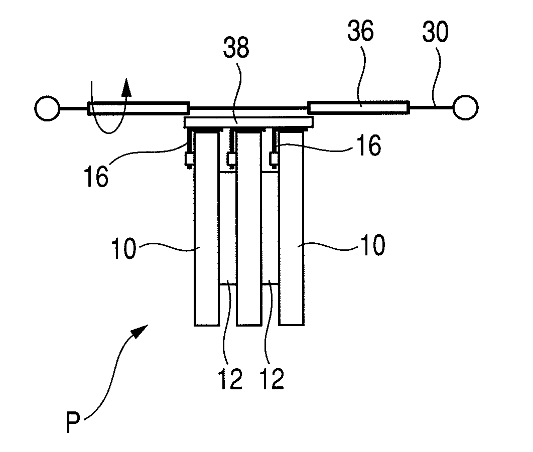
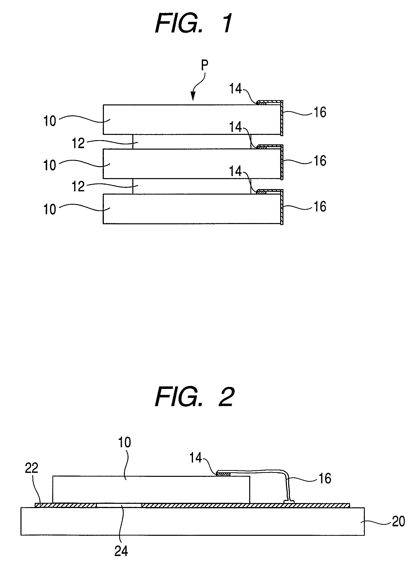
[0050]In this invention, first, as shown in FIG. 1, plural semiconductor elements 10, 10, 10 are stacked to form a stacked body P through adhesive layers 12.

[0051]In such a semiconductor element 10, a gold wire 16 serving as a metallic wire with its one end connected to an electrode terminal 14 formed on the one main surface is extended out to the side surface of the semiconductor element while being in contact therewith. In stacking these semiconductor elements 10, 10, 10 to form the stacked body P, the position of each semiconductor element 10 is adjusted so that the gold wire 16 extended out to the side surface of the semiconductor element is linearly arranged.

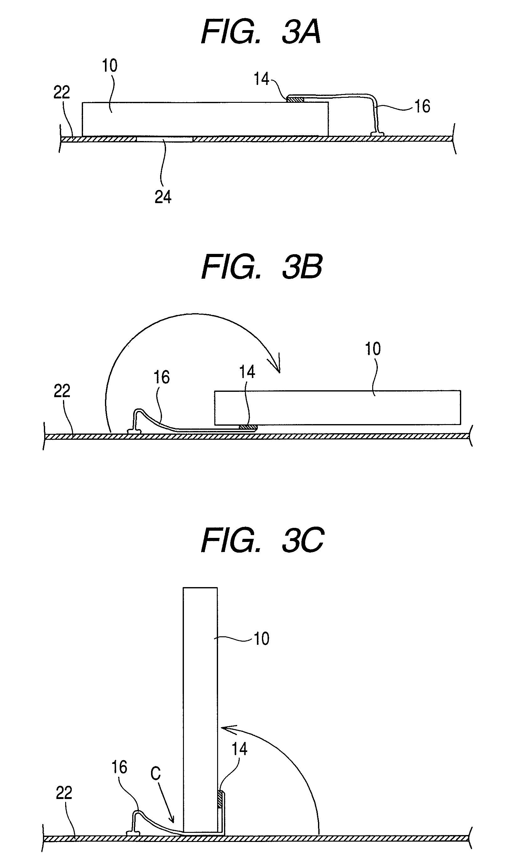
[0052]In order to form the semiconductor element 10 shown in FIG. 1, as shown in FIG. 2, a metallic foil 22 such as an aluminum foil is placed on a sucking plate 20 and the semiconductor element 10 is placed on a through-hole 24 made in the metallic foil 22. The semiconductor element 10 is placed on the metallic foil 22 so ...


PUM


Abstract

After plural semiconductor elements are stacked to form a stacked body P, side wirings are formed on the side surface of the stacked body P, thereby manufacturing a semiconductor apparatus in which the respective semiconductor elements are electrically connected to one another. In this case, as the semiconductor element, a semiconductor element 10 is employed in which a gold wire 16 with its one end connected to an electrode terminal of the semiconductor element is extended out to the side surface. A conductive paste 36 containing conductive particles applied over a predetermined length of a transferring wire 30 is transferred to the side surface of the stacked body P so that the gold wires 16 extended out to the side surfaces of the semiconductor elements 10, 10, 10 are connected, thereby forming the side wirings.

Description

BACKGROUND OF THE INVENTION[0001]This invention relates to a method for forming side wirings, and more particularly to a method for manufacturing a semiconductor apparatus in which plural semiconductor elements are stacked to form a stacked body and thereafter side wirings are formed on the side surface of the stacked body to electrically connect the semiconductor elements to one another.[0002]For example, the following Patent Reference 1 proposes the semiconductor apparatus in which plural semiconductor elements are stacked to form a stacked body and thereafter side wirings are formed on the side of the stacked body to electrically connect the semiconductor elements to one another.[0003]Such side wirings for the semiconductor apparatus, as shown in FIG. 14, can be formed in such a way that a conductive paste containing conductive particles is spit out from a nozzle 102 to form linear strips 104, 104, . . . of the conductive paste along the side surface of a stacked body A formed by...

Claims


Application Information

Patent Timeline
Patent Type & Authority Patents(United States)
IPC IPC(8): H01L21/44
CPCH01L21/6835H01L24/24H01L24/78H01L24/82H01L24/85H01L25/0657H01L24/45H01L2224/24145H01L2224/45144H01L2224/48091H01L2224/48465H01L2224/48471H01L2224/78H01L2224/85001H01L2225/06551H01L2225/06575H01L2924/01004H01L2924/01013H01L2924/01015H01L2924/01029H01L2924/01047H01L2924/01074H01L2924/01079H01L2924/30105H01L2924/00014H01L2924/01005H01L2924/01006H01L2924/01033H01L2924/00H01L2224/76152H01L24/48H01L2224/4554H01L23/12H01L23/48
Inventor MIZUNO, SHIGERUKURIHARA, TAKASHISHIRAISHI, AKINORIMURAYAMA, KEIHIGASHI, MITSUTOSHI
Owner SHINKO ELECTRIC IND CO LTD
Why Eureka
Try Eureka