Optical plate, method of manufacturing optical plate, backlight assembly and liquid crystal display device

a technology of optical plates and backlight assemblies, applied in the field of optical plates, can solve problems such as deteriorating image quality

Active Publication Date: 2010-10-26
SAMSUNG DISPLAY CO LTD
View PDF1 Cites 1 Cited by
  • Summary
  • Abstract
  • Description
  • Claims
  • Application Information

AI Technical Summary

Problems solved by technology

The brightness level of an LCD can be lowered by the diffusing agent, thereby deteriorating the image quality.

Method used


Image

  • Optical plate, method of manufacturing optical plate, backlight assembly and liquid crystal display device
  • Optical plate, method of manufacturing optical plate, backlight assembly and liquid crystal display device
  • Optical plate, method of manufacturing optical plate, backlight assembly and liquid crystal display device

Examples


Embodiment Construction

[0054]Hereinafter, exemplary embodiments of the present invention will be described with reference to the accompanying drawings. Like numerals may refer to similar or identical elements throughout the description of the figures.

[0055]A liquid crystal display device according to an exemplary embodiment of the present invention will be described with reference to FIGS. 1 through 3.

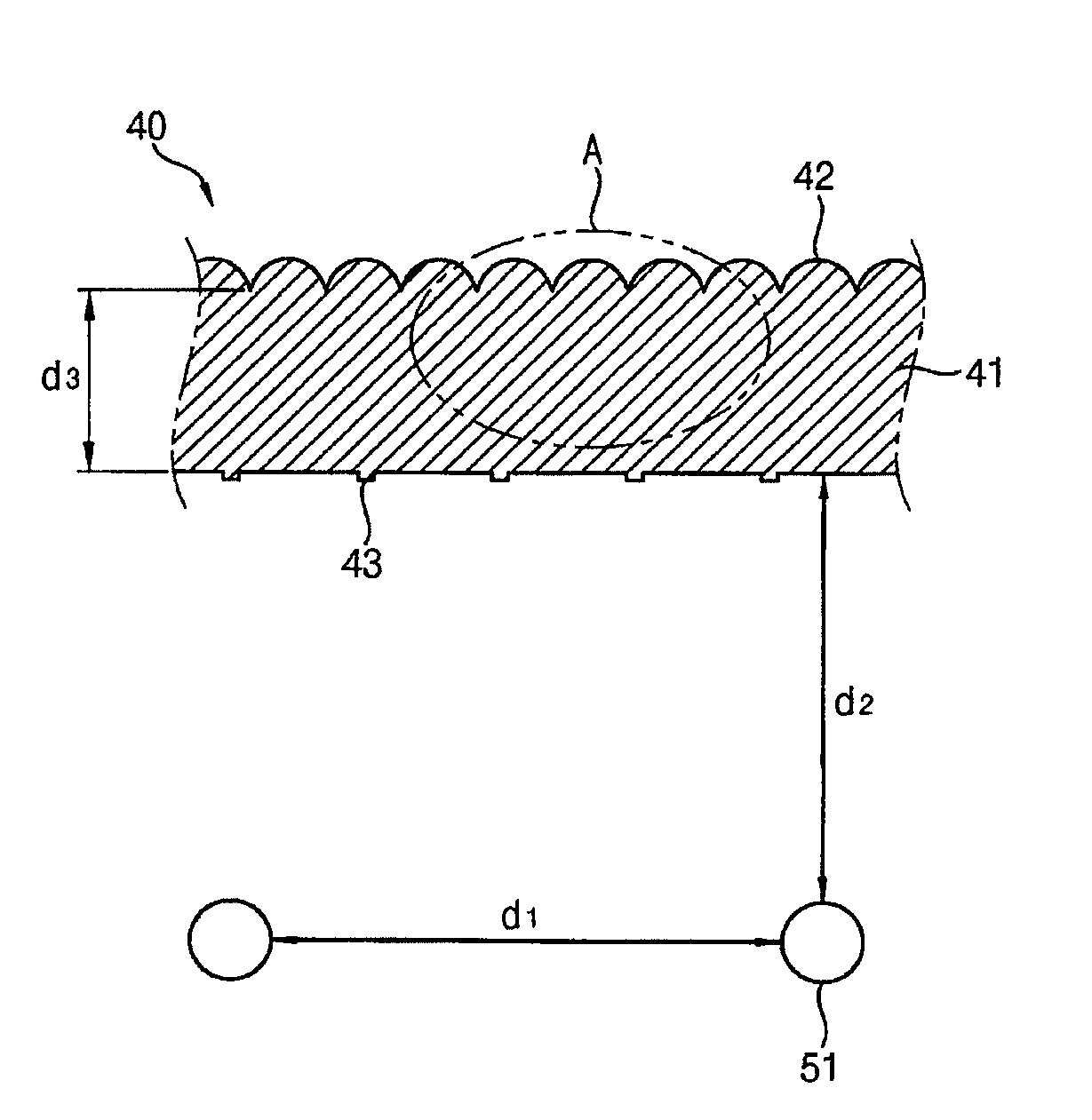
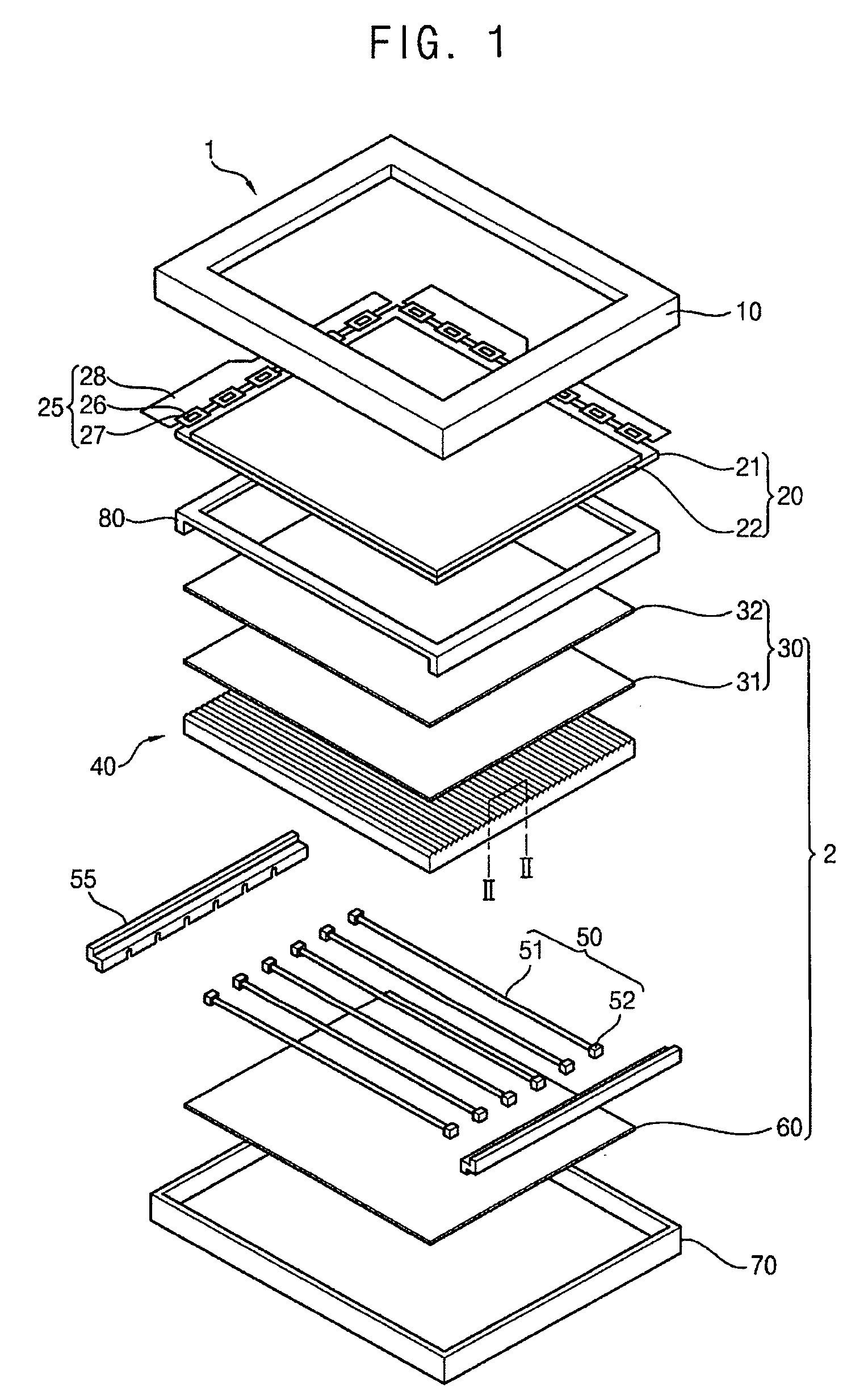
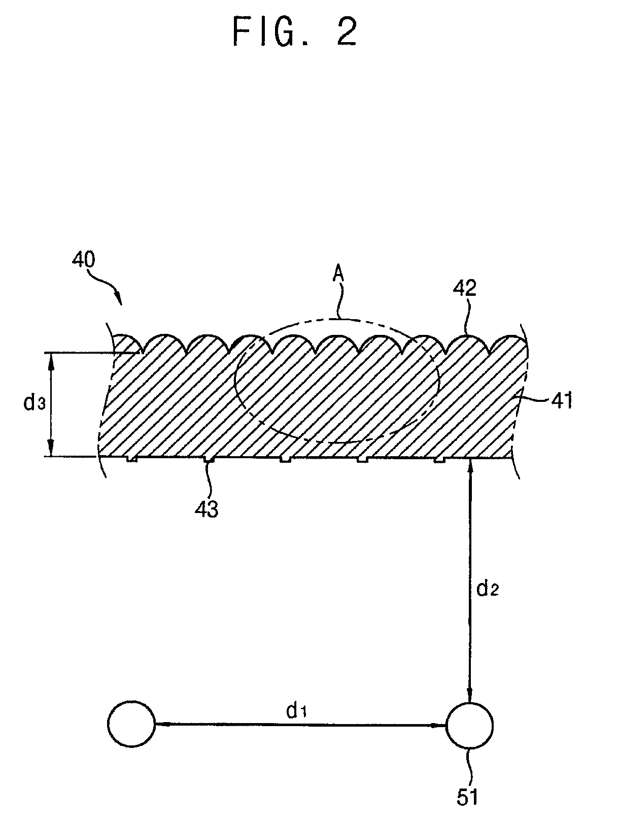
[0056]As shown in FIG. 1, a liquid crystal display device 1 includes a liquid crystal display panel 20 and a backlight assembly 2 supplying light to the liquid crystal display panel 20. The liquid crystal display panel 20 and the backlight assembly 2 are disposed between an upper cover 10 and a lower cover 70. The liquid crystal display panel 20 is disposed on a panel supporting mold 80.

[0057]The liquid crystal display panel 20 includes a first substrate 21 on which a plurality of thin film transistors are formed and a second substrate 22, which faces the first substrate 21. A liquid crystal layer (not shown...


PUM


Abstract

An optical plate includes a main body plate, and a plurality of lens patterns formed on a first surface of the main body plate, wherein the lens patterns are elongated in a first direction and arranged in parallel with each other in a second direction crossing the first direction, wherein a cross section of the lens patterns form a part of an ellipse shape, the ratio of a semi-major axis to a semi-minor axis of the ellipse shape ranging from about 1.65 to about 1.75.

Description

CROSS-REFERENCE TO RELATED PATENT APPLICATIONS[0001]This application is a continuation-in-part of U.S. patent application Ser. No. 11 / 746,702 filed on May 20, 2007, which claims priority to Korean Patent Application Nos. 2006-0041843, filed on May 10, 2006, and 2007-0021353, filed on Mar. 5, 2007, the disclosures of which are herein incorporated by reference in their entireties.BACKGROUND OF THE INVENTION[0002]1. Technical Field[0003]The present disclosure relates to an optical plate, a method of manufacturing an optical plate, a backlight assembly and a liquid crystal display device.[0004]2. Discussion of Related Art[0005]In general, a liquid crystal display device includes a liquid crystal display (LCD) panel and a light source. The LCD panel includes a first substrate having a plurality of thin film transistors, a second substrate facing the first substrate, and a liquid crystal layer interposed between the first and second substrates. The LCD panel does not generate light of its...

Claims


Application Information

Patent Timeline
Patent Type & Authority Patents(United States)
IPC IPC(8): F21V8/00
CPCG02B6/0038G02F1/133604G02B3/0012G02B6/0053G02F2001/133507G02F2001/133607G02F1/133507G02F1/133607
Inventor HA, JU-HWAPAEK, JUNG-WOOKCHOI, JIN-SUNGJOO, BYUNG-YUNKIM, JIN-SOOSONG, MIN-YOUNG
Owner SAMSUNG DISPLAY CO LTD
Why Eureka
Try Eureka