Quantum detector array

a detector array and quantum technology, applied in the field of photodetectors, can solve the problems of large size, high voltage, and large size of gamma-ray scattering, and achieve the effect of less reliable information about the distribution of gamma-ray sources in the patient's body, and large siz

Active Publication Date: 2010-11-02
SEMICON COMPONENTS IND LLC
View PDF22 Cites 5 Cited by
  • Summary
  • Abstract
  • Description
  • Claims
  • Application Information

AI Technical Summary

Benefits of technology

[0009]Other aspects of the invention, including devices, structures, assemblies, systems, arrays, meta-arrays, methods, and the like which constitute

Problems solved by technology

Scattered gamma-rays provide less reliable information about the distribution of gamma-ray sources in the patient's body than unscattered gamma-rays.
However, these conventional technologies also have disadvantages, such as large size, high voltage, sensitivity to ambient magnetic fields, comp

Method used


Image

  • Quantum detector array
  • Quantum detector array
  • Quantum detector array

Examples


Embodiment Construction

[0014]Reference will now be made in detail to the exemplary embodiments and methods of the invention as illustrated in the accompanying drawings, in which like reference characters designate like or corresponding parts throughout the drawings. It should be noted, however, that the invention in its broader aspects is not limited to the specific details, representative devices and methods, and illustrative examples shown and described in this section in connection with the exemplary embodiments and methods.

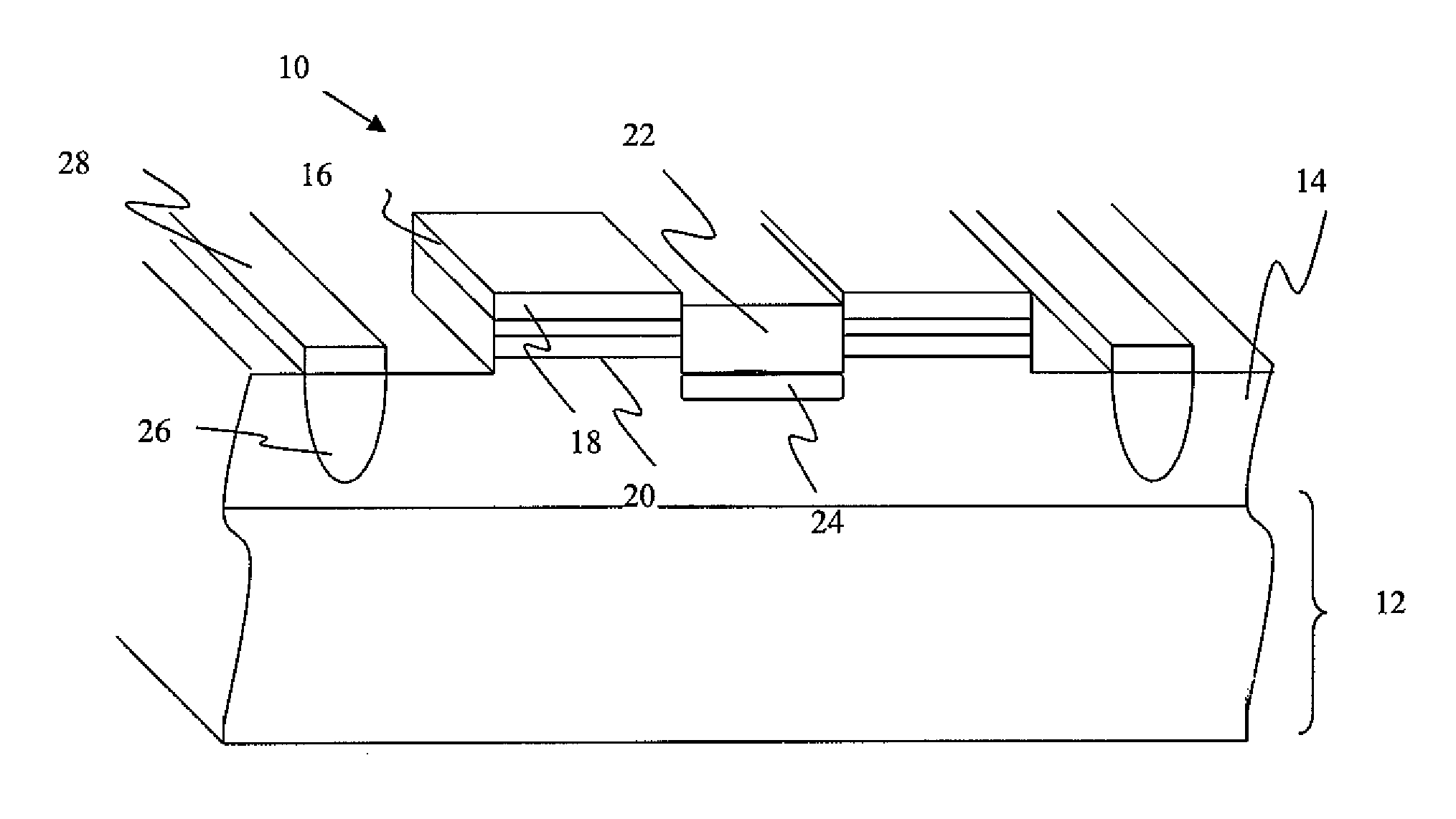
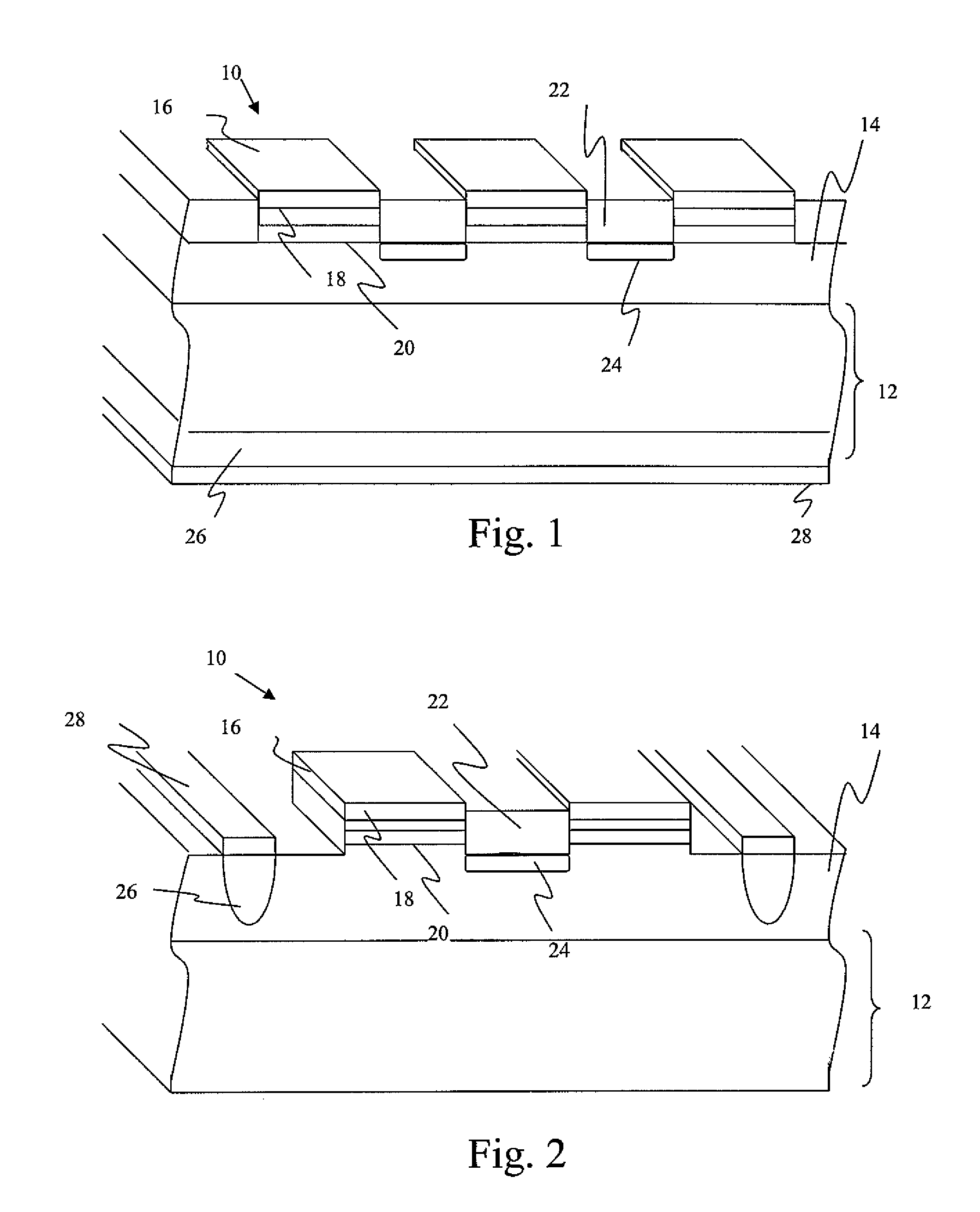
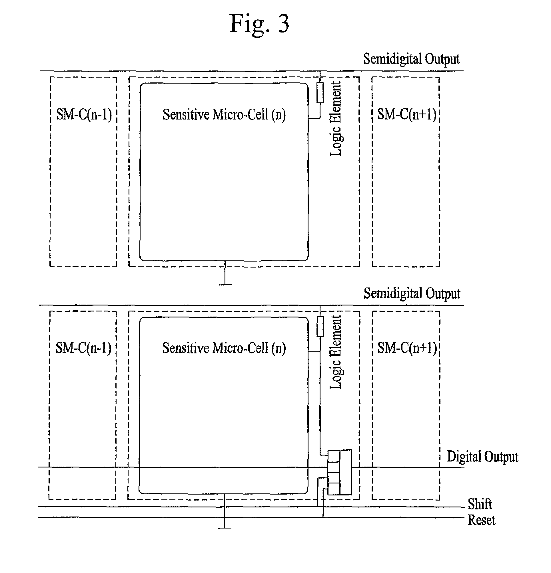
[0015]FIGS. 1 and 2 depict a binary quantum detector array according to exemplary embodiments of the invention.

[0016]The quantum photodetector arrays, generally designated by reference numeral 10 in FIGS. 1 and 30 in FIG. 2, present a realization of the binary quantum photodetector through the application of CMOS compatible and CMOS technology.

[0017]The semiconductor structure of binary quantum photodetector includes a semiconductor substrate 12 such as silicon or other semiconducto...


PUM


Abstract

A quantum detector array is provided. The array includes a semiconductor substrate and an epitaxial layer on the semiconductor substrate. The epitaxial layer includes a plurality of binary quantum sensor elements operable in breakdown mode to generate signals, logic elements, and a digital processing circuit. The binary quantum sensor elements each have a radiation-sensitive drift region and amplification region with a pn junction for detecting radiation from a radiation-emission source. The logic elements are each electrically interconnected to a corresponding binary sensor element of the plurality of binary quantum sensor elements for resetting the corresponding binary sensor element, generating digital information based on the signals received from the corresponding binary sensor element, and outputting the digital information. The digital processing circuit carries out digital processing of logic and time signals from the binary sensor elements.

Description

CROSS-REFERENCE TO RELATED APPLICATION(S)[0001]This patent application claims the benefit of priority of U.S. provisional application 60 / 960,812 filed on Oct. 15, 2007, the complete disclosure of which is incorporated herein by reference.FIELD OF THE INVENTION[0002]The present invention relates to photodetectors, including binary quantum photodetectors for converting photon flux into proportional semi-digital or digital electric signals with high efficiency and fidelity. The present invention further relates to devices, apparatus, systems, and methods of making and employing quantum photodetectors. The present invention possesses wide applicability, including in the fields of medical imaging, homeland security, and civilian and military applications involving the detection of low photon flux intensity.BACKGROUND OF THE INVENTION[0003]Photo detectors are employed in many applications requiring low intensity radiation detection, such as medical imaging systems (e.g., positron emission...

Claims


Application Information

Patent Timeline
IPC IPC(8): G01T1/24
CPCH01L27/1446H01L31/117
Inventor SAVELIEV, VALERI
Owner SEMICON COMPONENTS IND LLC
Why Eureka
Try Eureka