Intergrated circuit and a method of cache remapping

a technology of integrated circuits and caches, applied in the direction of memory adressing/allocation/relocation, error detection/correction, instruments, etc., can solve the problems of insufficient memory bandwidth, module faulty, and inability to meet the demand for memory bandwidth in recent high-performance vlsi processors, etc., to achieve less chip area and greater degree of freedom

Inactive Publication Date: 2010-11-02
NYTELL SOFTWARE LLC
View PDF17 Cites 389 Cited by
  • Summary
  • Abstract
  • Description
  • Claims
  • Application Information

AI Technical Summary

Benefits of technology

[0011]Accordingly, faulty modules can be remapped without limitations in order to optimise the utilization of the memory modules by providing an even distribution.
[0012]According to an aspect of the invention, the cache memory L2_BANK is implemented as a set-associative cache, resulting in a faster cache.
[0014]According to still a further aspect of the invention said remapping means performs the remapping on the basis of a reduction mapping. Accordingly, fewer elements are output than are input. Therefore, reduction mapping provides a greater degree of freedom for remapping faulty modules.
[0015]According to a preferred aspect of the invention, a Tag RAM unit TagRAM is associated to said cache and is used to identify, which data is cached in said cache memory L2_BANK. Furthermore, said remapping means is arranged in series with said Tag RAM unit TagRAM. Such an implementation is cheaper, since less chip area is required.
[0016]According to a further preferred aspect of the invention, a Tag RAM unit TagRAM is associated to said cache and is used to identify which data is cached in said cache memory L2_BANK. Furthermore, said remapping means is arranged in parallel to said Tag RAM unit TagRAM. This implementation is faster, since the remapping is performed in parallel to the Tag RAM.

Problems solved by technology

The increasing demand for memory bandwidth in recent high-performance VLSI processors is not satisfied by existing memory technology.
However, if a plurality of memory modules are used, some of these modules might be faulty.
Nonetheless, the teachings of Lu et al relate to the communication between processors and main memory having redundant memory modules without any caches between the processors and the main memory, which does not appear to be beneficial in terms of latency and bandwidth.
However, an increase in the circuit density is closely coupled with an increase in probability of defects.
However, since the provision of caches with spare or redundant memory modules is expensive, new techniques being able to sooth the degradation of cache performance without spare cache blocks are needed.
Many processing architectures can work without any cache but at the cost of degraded performance.
Therefore, introducing additional redundancy, like spare memory blocks, is inefficient.
All addresses are still cacheable, but conflict misses are increased.

Method used


Image

  • Intergrated circuit and a method of cache remapping
  • Intergrated circuit and a method of cache remapping
  • Intergrated circuit and a method of cache remapping

Examples


first embodiment

[0032]FIG. 3 depicts the select signal circuitry for the L2 cache according to a In FIG. 3 a tag RAM unit TagRAM, a remapping means RM, two registers R and a plurality of comparators C are shown in FIG. 3. The pipeline registers R receive the address Ad as input signal, while one register R provides a tag reference signal tag_ref as output, and the other register provides a bank selection signal bank_select and a word selection signal word_select as output. The tag RAM unit TagRAM receives the address Ad as input and outputs the signals tag0, . . . , tag5. These signals and the tag reference signal tag_ref are input signals of the comparators C, respectively, which output the hit signals hit0, . . . , hit5. These hit signals, the bank select signal bank_select and the word selection signal word_select are input to the remapping means RM, where the remapping operation is performed and the input signals are mapped to hit'0 , . . . hit'5, bank'select, and word_select representing the ...

second embodiment

[0036]The registers R in the second embodiment are not essential. The AND gates and OR gates occur 6*9 times and 9 times, respectively. However, this function may also be implemented for example using a multiplexer.

[0037]To further improve the performance of the selection circuitry according to the first and second embodiment, the cache hits and the cache line replacements should not target any faulty modules. In order to avoid this, a look-up table is preferably provided in the Tag RAM unit, but can also be implemented in the remapping unit RM or in the MAP RAM unit. The idea behind the look up table is to be able to avoid hits on all blocks of a faulty module, and furthermore to exclude such a module from being a replacement target. If the valid and lock bits are already implemented in a cache, the implementation of FIG. 5 is basically for free.

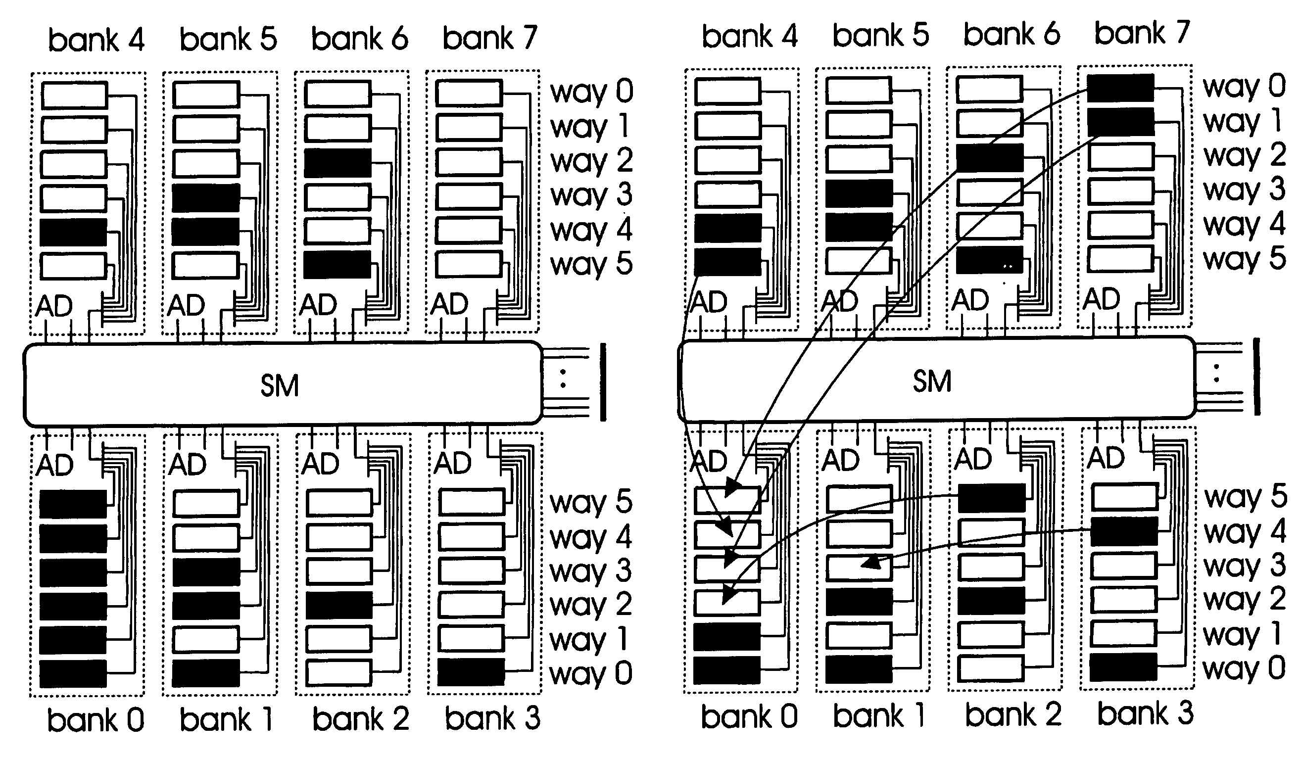
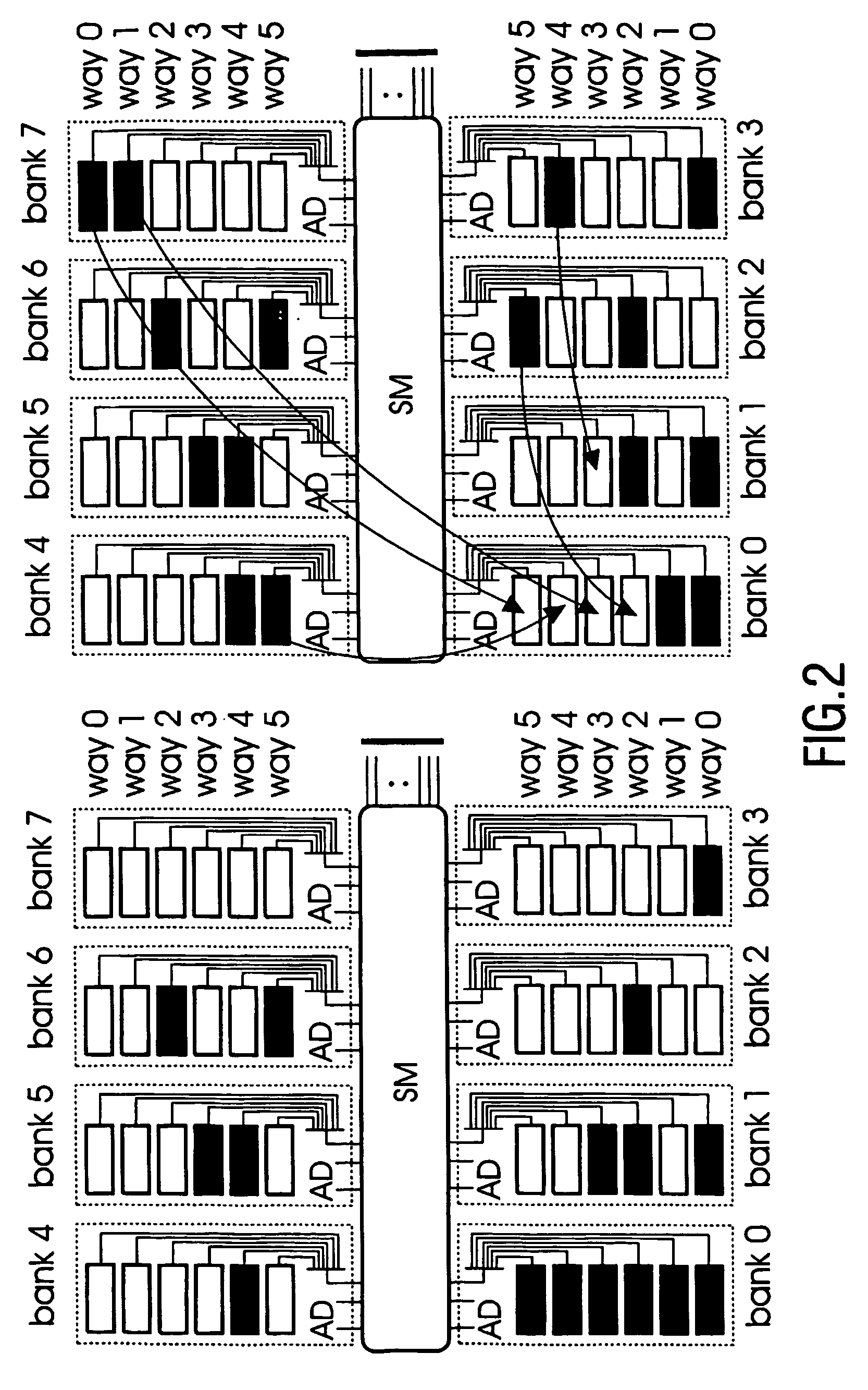
[0038]FIG. 5 shows a representation of such a table for a remapping according to FIG. 2. Faulty modules are marked as unusable by setting ...

fourth embodiment

[0041]In FIG. 6 a look-up table is shown, which represents a look up table of a combined map RAM and the tag RAM according to the Additionally, compared with the look up table according to FIG. 5, the table according to FIG. 6 comprises an extra column, i.e. the map column, for each way. This column contains the remapping information, e.g. the block at (index0,bank0,way2) gets remapped to (index0,bank2,way5), since the values 2 and 5 are written into the corresponding map field. In order to realise a cheap and fast implementation, a block is preferably not remapped to a different index, but merely to a new way and bank. However, the remapping may alternatively also be performed over several indexes.

[0042]The remapping means may comprise a programmable permutation unit which indicates the module-to-module mapping, a circuit using this permutation to reshuffle modules by recomputing module selects, and / or a mechanism to permanently invalidate the tag rams associated with a faulty mod...


PUM


Abstract

An integrated circuit is provided with at least one processing unit (TM), a cache memory (L2 BANK) having a plurality of memory modules, and remapping means (RM) for performing an unrestricted remapping within said plurality of memory modules. Accordingly, faulty modules can be remapped without limitations in order to optimise the utilization of the memory modules by providing an even distribution of the faulty modules.

Description

FIELD OF THE INVENTION[0001]The invention relates to an integrated circuit and a method of cache remapping.BACKGROUND OF THE INVENTION[0002]The increasing demand for memory bandwidth in recent high-performance VLSI processors is not satisfied by existing memory technology. In “Fault-Tolerant Interleaved Memory Systems with Two-Level Redundancy”, by Lu et al in IEEE Transactions on Computers, Vol. 46, No. 9, September 1997, several memory banks or modules of a main memory are accessed by processors in an interleaved fashion, in order to achieve a memory with high bandwidth. However, if a plurality of memory modules are used, some of these modules might be faulty. To cope with these faulty modules Lu et al proposes to use a memory containing a plurality of modules as well as to provide some spare modules in said memory. These spare modules may belong to the same bank or may constitute global spare modules. If a faulty module occurs, the memory management may initiate a replacement of ...

Claims


Application Information

Patent Timeline
Patent Type & Authority Patents(United States)
IPC IPC(8): G06F12/00G06F13/28G06F13/00G06F12/08G06F12/0846G06F12/0864G11C29/00
CPCG06F12/0864G11C29/76G06F12/0846G11C29/88
Inventor BINK, ADRIANUS JOSEPHUSSTRAVERS, PAUL
Owner NYTELL SOFTWARE LLC
Why Eureka
Try Eureka