Stacked semiconductor package electrically connecting semiconductor chips using outer surfaces thereof and method for manufacturing the same

a technology of electrical connection and semiconductor chips, which is applied in the direction of semiconductor devices, semiconductor/solid-state device details, electrical apparatus, etc., can solve the problems of complex manufacturing processes, difficult electrical connection of stacked semiconductor chips using through-electrodes, and marked increase in the volume of stacked semiconductor packages, so as to reduce the number of manufacturing processes and prevent damage

Active Publication Date: 2010-11-23
SK HYNIX INC
View PDF5 Cites 38 Cited by
  • Summary
  • Abstract
  • Description
  • Claims
  • Application Information

AI Technical Summary

Benefits of technology

[0008]Embodiments of the present invention include a stacked semiconductor package in which respective semiconductor chips are electrically connected using the outer surfaces of the semiconductor chips without forming conductive wires or through-electrodes, so that the volume of the stacked semiconductor package and the number of manufacturing processes can be decreased and the semiconductor chips are prevented from being damaged.

Problems solved by technology

This can be problematic because the volume of the stacked semiconductor package markedly increases when the spacers must be interposed between the semiconductor chips.
Electrically connecting the stacked semiconductor chips using the through-electrodes can be problematic as well.
That is, since through-holes having a fine size must be defined in the semiconductor chips and the through-electrodes must be formed in the through-holes, manufacturing processes are complicated and the semiconductor chips are likely to be damaged while defining or forming the through-holes or the through-electrodes in the semiconductor chips.

Method used


Image

  • Stacked semiconductor package electrically connecting semiconductor chips using outer surfaces thereof and method for manufacturing the same
  • Stacked semiconductor package electrically connecting semiconductor chips using outer surfaces thereof and method for manufacturing the same
  • Stacked semiconductor package electrically connecting semiconductor chips using outer surfaces thereof and method for manufacturing the same

Examples


first embodiment

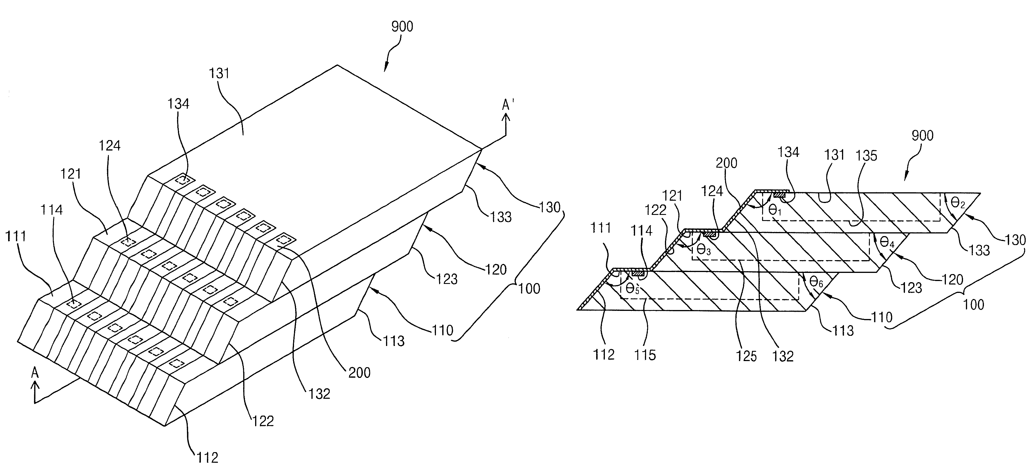
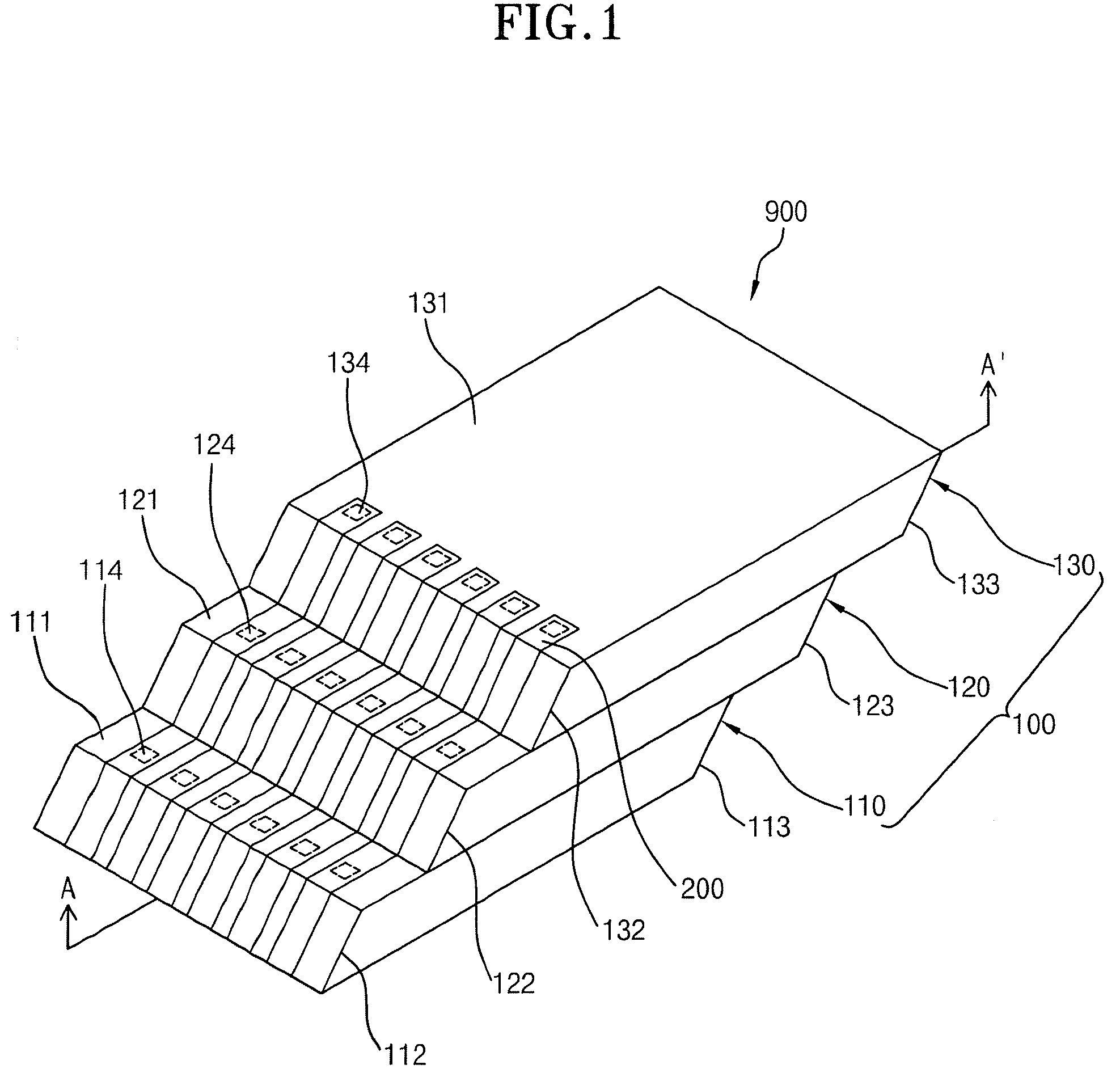
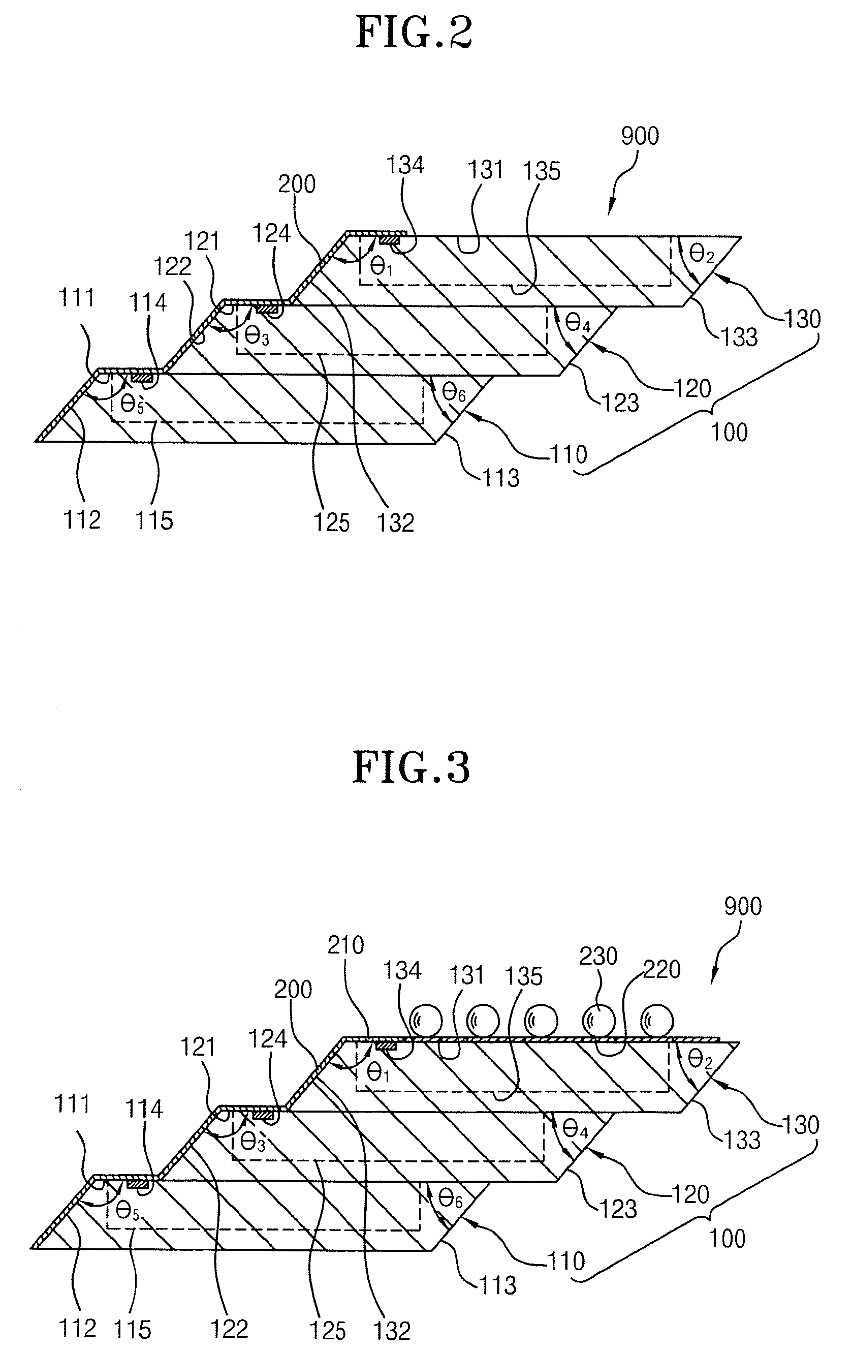
[0063]FIG. 1 is a perspective view showing a stacked semiconductor package in accordance with the present invention. FIG. 2 is a cross-sectional view of FIG. 1 along the line A-A′.

[0064]Referring to FIGS. 1 and 2, a stacked semiconductor package 900 includes a semiconductor chip module 100 and connection patterns 200.

[0065]The semiconductor chip module 100 includes a plurality of semiconductor chips 110, 120, and 130. For example, in the present embodiment, the semiconductor chip module 100 includes three semiconductor chips 110, 120, and 130.

[0066]Hereinbelow, the three semiconductor chips 110, 120, and 130 included in the semiconductor chip module 100 are defined as a first semiconductor chip 110, a second semiconductor chip 120, and a third semiconductor chip 130.

[0067]For example, in the present embodiment, the first through third semiconductor chips 110, 120, and 130 may comprise the same kind of semiconductor chips, having the same size and the same shape. Alternatively, at le...

fourth embodiment

[0101]FIG. 5 is a cross-sectional view showing a stacked semiconductor package in accordance with the present invention. The stacked semiconductor package according to this embodiment of the present invention is substantially the same as that shown in FIG. 4, except the embodiment as shown in FIG. 5 also includes a plurality of package modules and a gap fill member. Therefore, the same technical terms and reference numerals will be used to refer to the substantially same component parts, and detailed descriptions thereof will be omitted.

[0102]Referring to FIG. 5, a stacked semiconductor package 900 includes at least two semiconductor chip modules 100, connection patterns 200, a substrate 300, and a gap fill member 350.

[0103]In the present embodiment, each of the two or more semiconductor chip modules 100 include first through third semiconductor chips 110, 120, and 130 which are stacked to be staggered in the shape of steps. The connection patterns 200, which are formed in the shape...

seventh embodiment

[0126]FIG. 8 is a cross-sectional view showing a stacked semiconductor package in accordance with the present invention.

[0127]Referring toFIG. 8, a stacked semiconductor package 900 includes a semiconductor chip module 500 and connection patterns 600.

[0128]The semiconductor chip module 500 includes a plurality of semiconductor chips 510, 520, and 530. For example, in the present embodiment, the semiconductor chip module 500 includes three semiconductor chips 510, 520, and 530. Hereinbelow, the three semiconductor chips 510, 520, and 530 of the semiconductor chip module 500 are defined as a first semiconductor chip 510, a second semiconductor chip 520, and a third semiconductor chip 530.

[0129]For example, in the present embodiment, the first through third semiconductor chips 510, 520, and 530 may comprise the same kind of semiconductor chips, having the same shape (e.g., the shape of a trapezoid) and different sizes. Alternatively, the first through third semiconductor chips 510, 520...


PUM


Abstract

A stacked semiconductor package and a method for manufacturing the same. The stacked semiconductor package includes a semiconductor chip module having two or more semiconductor chips which are stacked in the shape of steps. Each of the semiconductor chips includes pads located on an upper surface thereof and an inclined side surface connected with the upper surface. Connection patterns are formed in the shape of lines on the inclined side surfaces and the upper surfaces of the semiconductor chips to electrically connect pads of the semiconductor chips.

Description

CROSS-REFERENCE TO RELATED APPLICATIONS[0001]The present application claims priority to Korean patent application number 10-2008-0062907 filed on Jun. 30, 2008, which is incorporated herein by reference in its entirety.BACKGROUND OF THE INVENTION[0002]The present invention relates generally to a stacked semiconductor package and a method for manufacturing same, and more particularly to a stacked semiconductor package electrically connecting semiconductor chips without requiring the formation of through-electrodes or connective wires, and reducing the size of the semiconductor package.[0003]Semiconductor chips suitable for storing and processing increasing amounts of data and semiconductor packages including such semiconductor chips have been developed.[0004]Recently stacked semiconductor packages, each including two or more stacked semiconductor chips, have been disclosed in the art in an effort to increase the data storage capacity and the data processing speed of semiconductor pac...

Claims


Application Information

Patent Timeline
Patent Type & Authority Patents(United States)
IPC IPC(8): H01L23/48
CPCH01L24/24H01L24/82H01L24/96H01L25/0657H01L23/49816H01L23/5389H01L2224/24145H01L2224/32145H01L2224/48091H01L2225/06551H01L2225/06555H01L2924/01047H01L2924/01075H01L2924/01078H01L2924/15311H01L2924/15331H01L2924/1815H01L2924/00014H01L2924/01005H01L2924/01006H01L2924/01033H01L2924/014H01L2224/48227H01L2225/06562H01L23/12
Inventor OH, TAC KEUN
Owner SK HYNIX INC
Why Eureka
Try Eureka