Silicon based thin film solar cell

a thin film solar cell and silicon technology, applied in the direction of basic electric elements, electrical apparatus, semiconductor devices, etc., can solve the problems of increasing facility costs, increasing production tact, and increasing production costs, so as to maintain a series resistance of the solar cell, reduce the cost, and reduce the cost

Inactive Publication Date: 2010-12-07
KANEKA CORP
View PDF16 Cites 5 Cited by
  • Summary
  • Abstract
  • Description
  • Claims
  • Application Information

AI Technical Summary

Benefits of technology

[0015]Taking the above situations into consideration, by disposing a layer having a lower refractive index compared with that of a photoelectric conversion layer, on a backside of the photoelectric conversion layer observed from a light incident side, without using different facilities from those for formation of the photoelectric conversion layer, the present invention aims at providing a silicon based thin film solar cell, efficiently and at a low cost, that can exhibit sufficient light trapping effect and can keep a series resistance of the solar cell smaller even if a layer having a low refractive index is disposed.
[0017]The silicon based low refractive index layer has a function to generate a diffusion potential in the photoelectric conversion layer, which is a layer doped with impurity to give a p type or an n type. In order to effectively reflect light on a surface thereof to the photoelectric conversion layer side, and to keep absorption loss of light in the layer as small as possible, the silicon based low refractive index layer preferably has a refractive index of not more than 2.5 at a wavelength of 600 nm, and has a thickness of not less than 300 angstroms.
[0018]A silicon based low refractive index layer is an alloy layer comprising silicon and elements, such as oxygen, typically a silicon oxides, preferably a ratio of a most abundantly existing constituent element, excluding silicon, in the layer is not less than 25 atom %, and the layer is preferably formed by methods, such as a high frequency plasma CVD that are same kind as methods for a photoelectric conversion layer. The silicon based low refractive index layer preferably includes crystalline silicon components in the layer, in order to reduce a resistance in a thickness direction of the layer itself.
[0020]In order to solve problems of increase in a series resistance of a solar cell caused by disposition of a silicon based low refractive index layer in a backside of a photoelectric conversion layer, the present inventors wholeheartedly investigated structures for optimal solar cells. As a result, it was found out that by disposing a thin silicon based interface layer in a backside of a silicon based low refractive index layer, a contact resistance to a back electrode layer comprising metal oxide layer disposed in a backside thereof was improved, and thereby a series resistance of the solar cell became smaller and conversion efficiency was improved.
[0021]In the present invention, a silicon based interface layer disposed between a silicon based low refractive index layer and a back electrode layer has small contact resistances with either of the silicon based low refractive index layer and the back electrode layer, and as a result a small series resistance of the solar cell is believed to be realized. Especially, as shown in FIG. 1, when silicon oxide is used as a silicon based low refractive index layer, and an amount of oxygen in the layer is increased to lower a refractive index to not more than 2.5, it is difficult to lower a contact resistance between the silicon based low refractive index layer and the back electrode layer. However, such a problem is solved by inserting a silicon based interface layer. Therefore, this technique enables design of the silicon based low refractive index layer to an optimal thickness and an optimal refractive index for light trapping. Furthermore, since simple change of film-forming conditions permits adjustment of a refractive index of the silicon based low refractive index layer, increase in light trapping effect by more delicate optical designs can also be expected, such as periodic variation of a refractive index in a thickness direction.
[0025]An n type silicon based interface layer 4n is formed on the n type silicon based low refractive index layer 4on. Crystalline silicon is mainly used for the n type silicon based interface layer 4n. The n type silicon based interface layer 4n is used in order to improve a contact resistance between the n type silicon based low refractive index layer 4on and a back electrode 5, and thus preferably has a thickness as small as possible in order to minimize light absorption loss in this layer. Specifically, the thickness is not more than 150 angstroms, and more preferably not more than 100 angstroms. Furthermore, as the n type silicon based interface layer 4n, a layer having an electric conductivity of about 1 to 102 S / cm is used. The n type silicon based interface layer 4n may include any one or more elements of oxygen, carbon, and nitrogen in a range not increasing a contact resistance with the back electrode 5.

Problems solved by technology

Although a thicker photoelectric conversion layer is more preferable for light absorption, a layer thicker than necessary may cause results of increasing cost for film-forming and time for production.
However, these conductivity type layers are inert layers not directly contributing to photoelectric conversion, and thus light absorbed with impurity doped in the conductivity type layer gives loss not contributing to generation of electric power.
However, since the zinc oxide film is formed by a technique of sputtering, spraying, etc., different facilities from that for semiconductor thin film formed in general by plasma CVD methods etc. are required, leading to occurrence of problems of facility cost rise and longer production tact.
Furthermore, there may occur problems that especially use of sputtering method in formation of the zinc oxide film may cause performance reduction by sputter damage to a ground semiconductor thin film.
Specifically, in Examples, a thickness of a-SiON (a-SiO) layer set thin as 200 angstroms does not permit expectation of sufficient light trapping effect.
However, this official report fails to describe about a refractive index of the obtained film, and fails to describe that the film can be disposed on a backside of a photoelectric conversion layer of the solar cell observed from a light incident side.
However, only simple use of the silicon oxide as an n type layer increased a series resistance of the solar cell, leading to a problem of reduction of conversion efficiency.
Thus, conventional technique cannot solve a problem of series resistance of solar cells that is believed to be caused by a contact resistance generated between a silicon based low-refractive index layer represented by silicon oxides, and a back electrode.

Method used


Image

  • Silicon based thin film solar cell
  • Silicon based thin film solar cell
  • Silicon based thin film solar cell

Examples


example 1

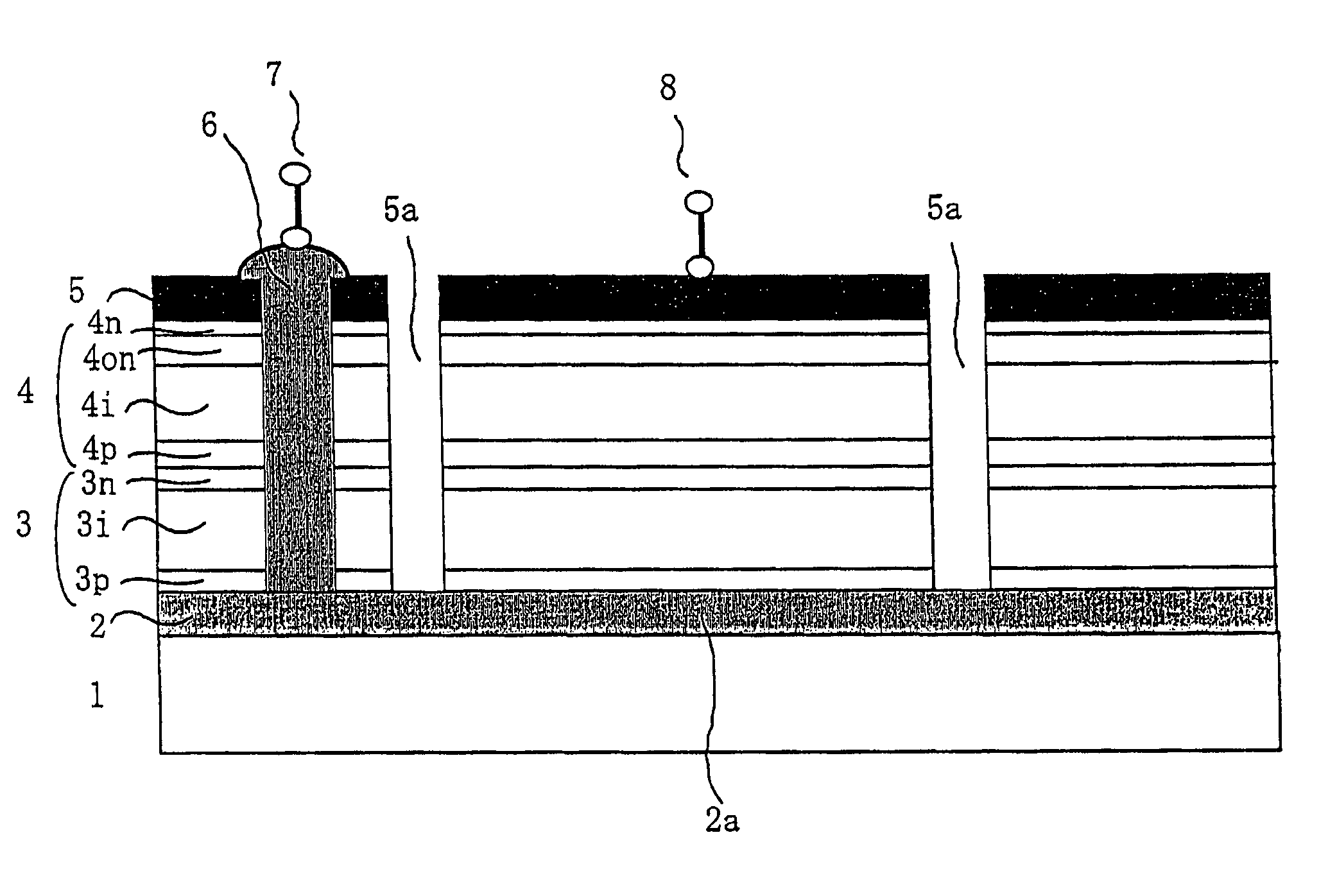
[0035]FIG. 3 is a sectional view showing schematically a hybrid thin film solar cell produced in each Example and each Comparative Example.

[0036]First, a transparent electrode layer 2 consisting of SnO2 and having a minute uneven structure on a surface thereof was formed by a heat CVD method on a principal surface of a translucent board 1 consisting a blue plate glass of a thickness of 0.7 mm.

[0037]Next, in order to form an amorphous photoelectric conversion unit 3, the translucent board 1 having a transparent electrode layer 2 formed thereon was introduced in a high frequency plasma CVD device. After the equipment was heated up to a predetermined temperature, an amorphous p type silicon carbide layer 3p with a thickness of 160 angstroms, a non doped amorphous i type silicon photoelectric conversion layer 3i with a thickness of 3000 angstroms, and an n type silicon layer 3n with a thickness of 300 angstroms were sequentially laminated.

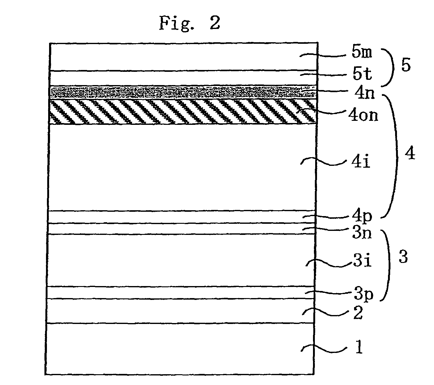
[0038]Furthermore, in order to form a crystallin...

example 2

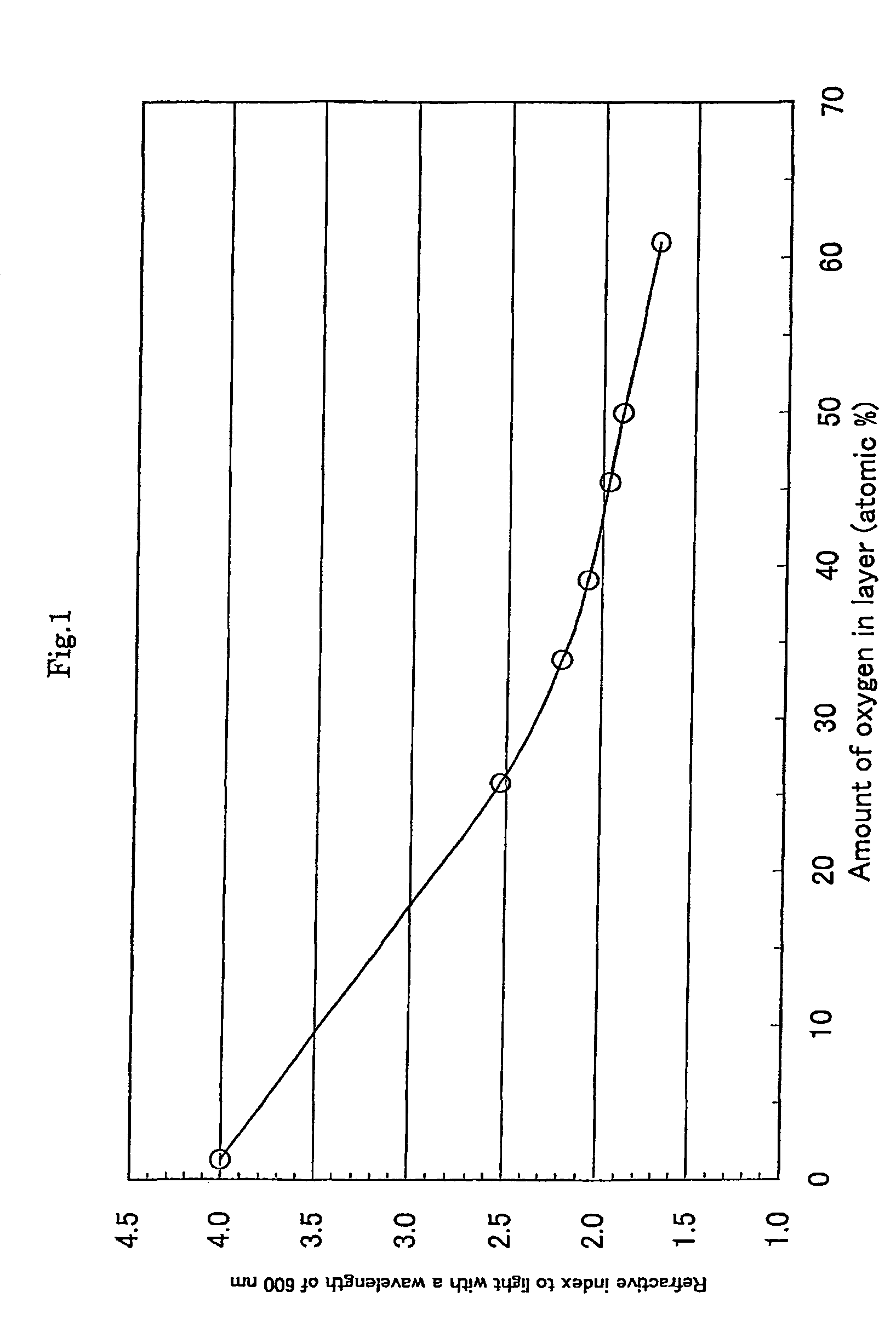
[0043]In Example 2, an almost similar process as in Example 1 was carried out except for having varied a refractive index at a wavelength of 600 nm in a range of 1.65 to 2.65 by varying only film-forming conditions of an n type silicon based low refractive index layer 4on. FIG. 5 shows a relationship between refractive indexes of the silicon based low refractive index layer, and conversion efficiency of the hybrid thin film solar cell.

example 3

[0044]In Example 3, an almost similar process as in Example 1 was carried out except for having varied a thickness of an n type silicon based low refractive index layer 4on in a range of 100 angstroms to 1000 angstroms. FIG. 6 shows a relationship between a thickness of the silicon based low refractive index layer and obtained conversion efficiency of the hybrid thin film solar cell.


PUM


Abstract

According to the present invention, sufficient light trapping effect can be exhibited and series resistance can be kept small, by sequentially forming a silicon based low refractive index layer and a thin silicon based interface layer on a backside of a photoelectric conversion layer observed from a light incident side, and as a result a silicon based thin film solar cell may be provided efficiently and at low cost.

Description

[0001]This application is a national phase of PCT application PCT / JP2004 / 010248 filed on Jul. 12, 2004, claiming priority to Japanese Application Nos. 2003-279491 filed on Jul. 24, 2003 and 2003-358362 filed Oct. 17, 2003, the entirety of which are incorporated by reference.TECHNICAL FIELD[0002]The present invention relates to a silicon based thin film solar cell, and in particular to a thin film solar cell enabling demonstration of light trapping effect by disposing a layer having a smaller refractive index than a refractive index of the photoelectric conversion layer on a backside of a photoelectric conversion layer observed from a light incident side.BACKGROUND ART[0003]In recent years, various thin film solar cells have come into use, in addition to conventional amorphous thin film solar cells, crystalline thin film solar cells are also being developed, and moreover hybrid thin film solar cells obtained by laminating these solar cells together are also put in practical use.[0004...

Claims


Application Information

Patent Timeline
Patent Type & Authority Patents(United States)
IPC IPC(8): H01L31/00H01L31/0216H01L31/042H01L31/052H01L31/06H01L31/075H01L31/076H01L31/077
CPCH01L31/075H01L31/076H01L31/056H01L31/077Y02E10/548Y02E10/52Y02E10/547H01L31/0445
Inventor SAWADA, TORUKOI, YOHEISASAKI, TOSHIAKIYOSHIMI, MASASHIGOTO, MASAHIROYAMAMOTO, KENJI
Owner KANEKA CORP
Why Eureka
Try Eureka