Electronic component

a technology of electroconductive resin and component, applied in the field of electroconductive components, can solve the problems of insufficient inhibition of cracks at the joining portion, easy cracks occurrence, etc., and achieve the effects of good cross-linked structure, good cross-linked structure, and good cross-linked structur

Active Publication Date: 2010-12-07
TDK CORPARATION
View PDF33 Cites 18 Cited by
  • Summary
  • Abstract
  • Description
  • Claims
  • Application Information

AI Technical Summary

Benefits of technology

[0008]Accordingly, the present invention has been accomplished with the view of the circumstance, and aims to provide an electronic component capable of reducing the occurrence of cracks at a joining portion with a board etc.
[0010]The electroconductive resin layer included in the external electrode is one containing the epoxy resin hardened product including an epoxy compound having a molecular weight of 2000 or more as the base compound. Such epoxy resin hardened product has a reasonably small ratio of a cross-linked structure formed in the hardened structure, because the base compound being the raw material thereof has a long molecular chain. Consequently, the epoxy resin hardened product has such property as being flexible. Thus, the electroconductive resin layer including the epoxy resin hardened product also becomes flexible, as compared with a case where a layer includes an epoxy resin hardened product using an epoxy compound having a molecular weight of less than 2000 as the base compound. Accordingly, even when the electronic component of the invention is subjected to thermal shock in such state that it is mounted on the board by the soldering of the external electrode etc., the stress added to the joining portion caused by the difference in the volume alteration relative to the board is relaxed sufficiently by the flexible electroconductive resin layer in the external electrode. As the result, the electronic component of the invention hardly generates cracks at the joining portion with the board.
[0011]In the electronic component of the invention, more preferably the epoxy resin further includes phenol resin as a hardening agent. Hereby, the epoxy resin hardened product is led to have a good cross-linked structure in the structure thereof, and, as the result, the stress relaxation properties of the electroconductive resin layer becomes further excellent.
[0012]It is further preferred when the epoxy compound is a linear bifunctional epoxy compound having an epoxy group at both ends. This results in a further good reduction in the ratio of the cross-linked structure in the epoxy resin hardened product, and further improvement of the flexibility of the electroconductive resin layer including the epoxy resin hardened product, because the molecular chain itself of the base compound can be flexible.

Problems solved by technology

However, the result of the study by the present inventors revealed that, when thermal shock is added to a board on which the electronic component has been mounted etc., since the board and the electronic component have large difference in the degree of expansion and contraction by heat, stress concentrates at the soldered joining portion of them to lead to easy occurrence of cracks.
Further, the occurrence of the crack at the joining portion could not sufficiently been inhibited often even when such laminated ceramic capacitor as described in the conventional document, in which the occurrence of the crack in an element assembly is reduced, was applied.

Method used


Image

  • Electronic component
  • Electronic component
  • Electronic component

Examples


example 1

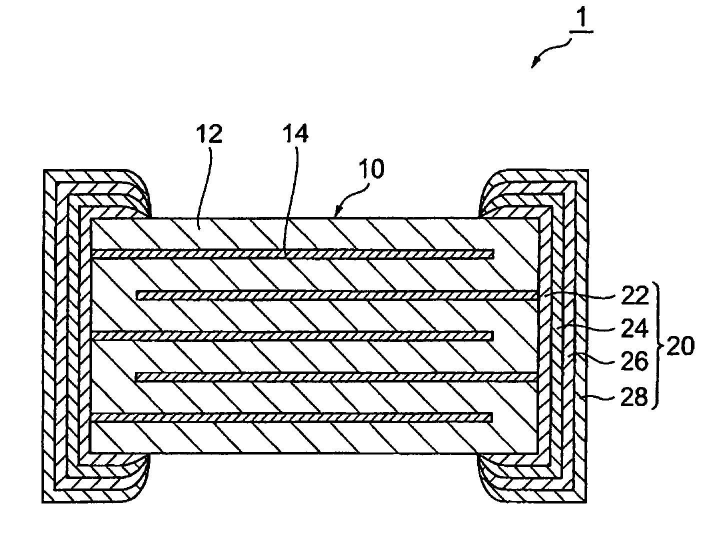
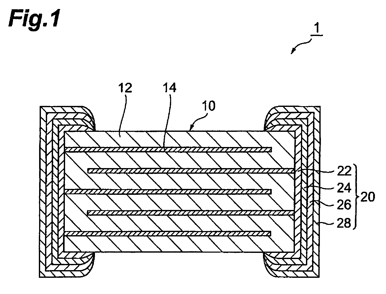
[0044]Firstly, an element assembly, in which a dielectric layer composed of barium titanate and an internal electrode layer composed of nickel were alternately arranged so that the dielectric layer lied on both outsides, was prepared. Next, on a pair of end faces facing to each other in the element assembly, an electroconductive paste containing Cu, glass frit and ethyl cellulose as an organic binder was coated, which was then calcined at 800° C. to form a first electrode layer on both end faces of the element assembly.

[0045]Next, on the surface of the first electrode layer, an electroconductive paste, which included 35% by weight of granular Ag powder having an average grain diameter of 1 μm, 35% by weight of flake-shaped Ag powder having an average grain diameter of 10 μm, 10% by weight of bisphenol-A type epoxy resin (base compound) having a molecular weight of 2900, 2% by weight of novolac type phenol resin hardening agent), and 18% by weight of butylcarbitol (solvent), was coat...

example 2

[0047]A capacitor was obtained in the same way as in Example 1 except that, as the electroconductive paste for forming the second electrode layer, a paste including 33.7% by weight of granular Ag powder having an average grain diameter of 1 μm, 33.7% by weight of flake-shaped Ag powder having an average grain diameter of 10 μm, 9.6% by weight of bisphenol-A type epoxy resin (base compound) having a molecular weight of 3800, 1.9% by weight of novolac type phenol resin (hardening agent) and 21.1% by weight of butylcarbitol (solvent) was used.


PUM

PropertyMeasurementUnit
temperatureaaaaaaaaaa
grain diameteraaaaaaaaaa

Abstract

The present invention aims to provide an electronic component capable of reducing the occurrence of cracks at the joining portion with a board etc. A capacitor 1 (laminated ceramic capacitor) being one example of the electronic component of the present invention is provided with an element assembly 10 (ceramic) and a pair of external electrodes 20 formed on both side surfaces of the element assembly. In the element assembly 10, a dielectric layer 12 and an internal electrode 14 are laminated alternately. The external electrode 14 has such constitution that a first electrode layer connected with the internal electrode 14, a second electrode layer (electroconductive resin layer) including a hardened product of epoxy resin containing an epoxy compound having a molecular weight of 2000 or more and plural epoxy groups as the base compound, a third electrode layer composed of Ni and a fourth electrode layer composed of Sn are formed in this order from the element assembly side.

Description

BACKGROUND OF THE INVENTION[0001]1. Field of the Invention[0002]The present invention relates to an electronic component, in particular to an electronic component using a ceramic material.[0003]2. Related Background of the Invention[0004]Many of electronic components such as a capacitor and inductor using a ceramic material have constitution that is provided with an element assembly composed of a ceramic material, an internal electrode provided inside the element assembly, and an external electrode provided on the surface of the element assembly so as to be connected with the internal electrode. For the electronic components, conventionally, methods have been studied for inhibiting cracks etc. of the element assembly that occur due to the difference between physical properties of the element assembly and the external electrode.[0005]For example, JP-A-11-219849 describes that, in a laminated ceramic capacitor being an example of the electronic component having the aforementioned stru...

Claims


Application Information

Patent Timeline
Patent Type & Authority Patents(United States)
IPC IPC(8): H01L21/02H01G4/12H01G4/30
CPCH01G4/2325H01G4/30H01L41/047H10N30/872H10N30/878G06K19/07732G06F2212/2146
Inventor KOMATSU, TAKASHITANABE, KOUJI
Owner TDK CORPARATION
Why Eureka
Try Eureka