Semiconductor integrated circuit for communication

a technology of integrated circuits and semiconductors, applied in the field of semiconductor integrated circuits for communication, can solve problems such as yield degradation, and achieve the effects of preventing the degradation of transmission characteristics, high yield, and reducing the risk of carrier leakag

Active Publication Date: 2010-12-07
RENESAS ELECTRONICS CORP
View PDF12 Cites 6 Cited by
  • Summary
  • Abstract
  • Description
  • Claims
  • Application Information

AI Technical Summary

Benefits of technology

[0006]The inventors of the present invention have examined a semiconductor integrated circuit for communication having therein a modulation circuit constructed by an NPN bipolar transistor and an MOSFET (Metal Oxide Semiconductor Field Effect Transistor) obtained by eliminating a PNP bipolar transistor from a modulation circuit using the PNP bipolar transistor for passing constant current in order to reduce the cost of a semiconductor integrated circuit for communication for a cellular phone having the function of dealing a signal according to the GSM.
[0013]The present invention has been achieved in the background as described above, and an object of the invention is to provide a semiconductor integrated circuit (RF IC) for communication realizing high yield without deteriorating the carrier leak characteristic even when a modulation circuit is constructed by using cheap parts with large variations.
[0018]Since the DC offset in the input circuit can be cancelled by the above-described means, occurrence of a carrier leak in the mixer at the post stage can be avoided, and degradation of the transmission characteristics can be prevented.
[0020]According to the present invention, a semiconductor integrated circuit (RF IC) realizing high yield without deteriorating the carrier leak characteristic even when a modulation circuit is constructed by using cheap parts with large variations can be realized.

Problems solved by technology

As a result, the inventors have found that the modulation circuit using no PNP bipolar transistor has a problem such the characteristic degradation called a carrier leak occurs conspicuously, and the yield deteriorates.
The carrier leak is a problem such that a frequency component of a carrier wave is included in a transmission signal due to a DC offset of the modulation circuit.

Method used


Image

  • Semiconductor integrated circuit for communication
  • Semiconductor integrated circuit for communication
  • Semiconductor integrated circuit for communication

Examples


Embodiment Construction

[0032]An embodiment of the present invention will be described by using the drawings.

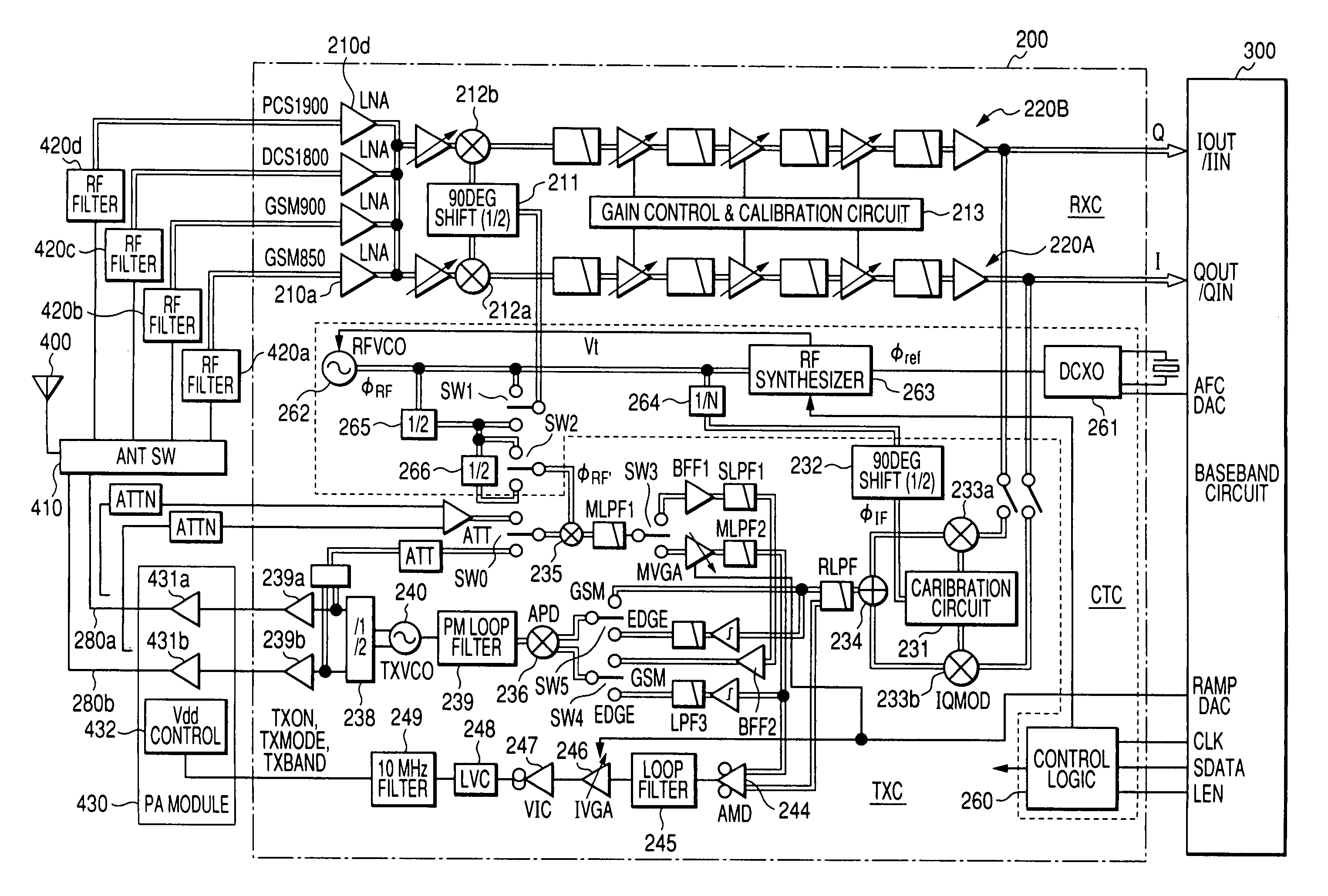
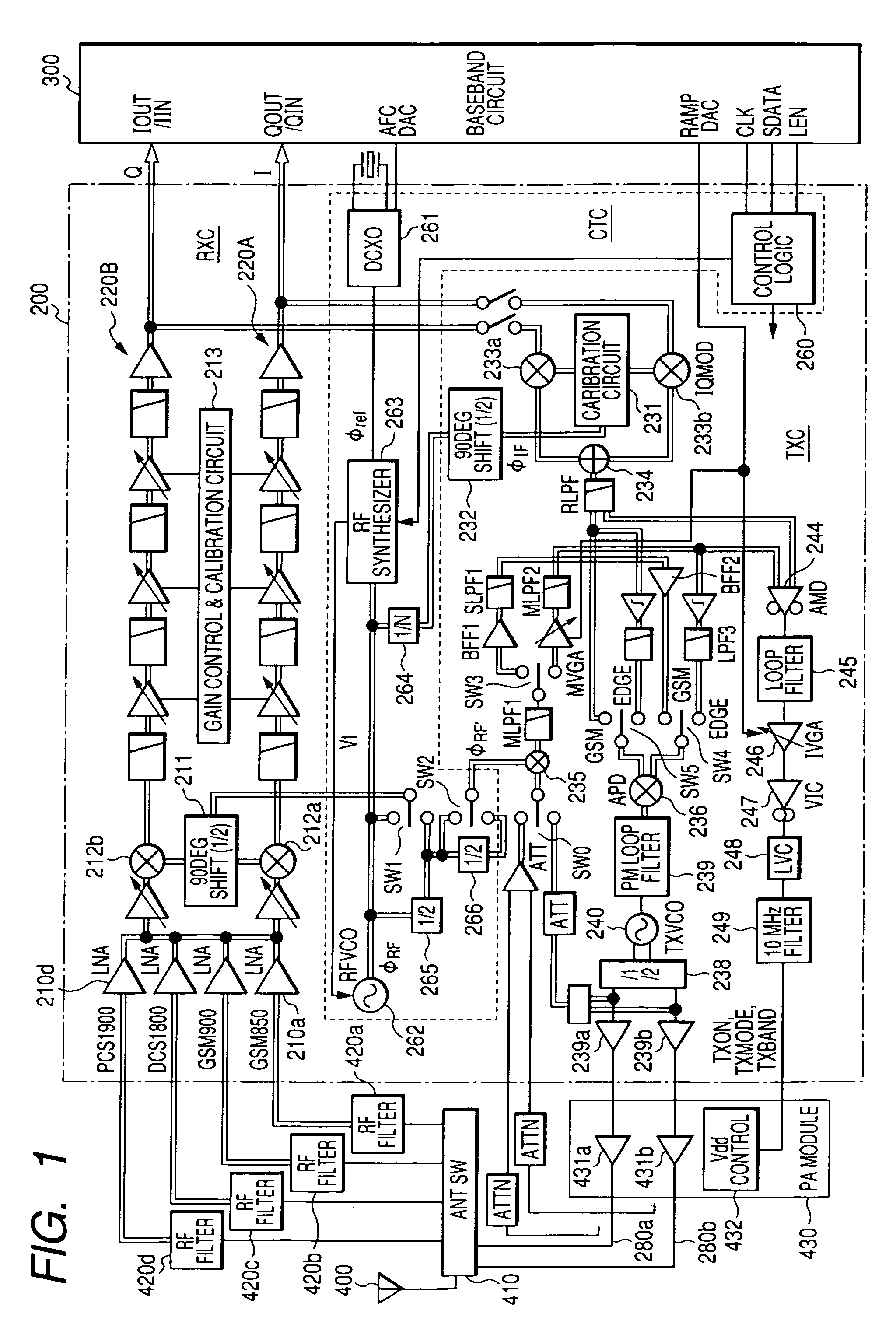
[0033]FIG. 1 shows an example of a semiconductor integrated circuit (RF IC) for communication to which the invention is applied and a radio communication system using the RF IC.

[0034]As shown in FIG. 1, the system includes an antenna 400 for transmitting / receiving signal waves, a switch 410 for switching transmission / reception, high frequency filters 420a to 420d each taking the form of an SAW filter or the like for eliminating an unnecessary wave from a reception signal, a radio frequency power amplifier (power module) 430 for amplifying a transmission signal, an RF IC 200 for demodulating a reception signal and modulating a transmission signal, and a baseband circuit 300 for performing a baseband process such as conversion of a sound signal and a data signal to be transmitted into an I signal of an in-phase component and a Q signal of a quadrature component with respect to a fundamental wave, and ...


PUM


Abstract

The present invention provides a semiconductor integrated circuit for communication (RF IC) realizing high yield without deteriorating a carrier leak characteristic even when a modulation circuit is formed by using cheep parts with large variations. In a semiconductor integrated circuit (RF IC) including: an input circuit constructed by a differential amplifier circuit and a level shifter, which is provided on the ante stage of a mixer of a differential circuit called a Gilbert Cell; and a modulation circuit that performs modulation by adding an I / Q signal and a carrier wave signal, a calibration circuit for canceling a DC offset in an output of the input circuit is provided.

Description

CROSS-REFERENCE TO RELATED APPLICATION[0001]The present application claims priority from Japanese patent application No 2005-052288 filed on Feb. 28, 2005, the content of which is hereby incorporated by reference into this application.BACKGROUND OF THE INVENTION[0002]The present invention relates to a semiconductor integrated circuit for communication having therein a modulation circuit for modulating a carrier wave signal with a transmission baseband signal and, further, to a technique for cancelling a DC offset of a modulation circuit. More particularly, the invention relates to a technique effectively applied to a semiconductor integrated circuit for communication which is mounted on a radio communication system such as a cellular phone having a mode of modulating only a phase component and a mode of modulating a phase component and an amplitude mode.[0003]In a radio communication system such as a cellular phone, a semiconductor integrated circuit for communication (hereinbelow, ...

Claims


Application Information

Patent Timeline
Patent Type & Authority Patents(United States)
IPC IPC(8): H04B1/04H04B1/00
CPCH03C3/40H03D3/007H03D7/1433H04B1/406
Inventor FURUYA, RYOJIOKADA, KAZUHISAMATSUI, HIROAKI
Owner RENESAS ELECTRONICS CORP
Why Eureka
Try Eureka