Semiconductor device, manufacturing method of semiconductor device, and display device

a semiconductor and semiconductor technology, applied in the direction of semiconductors, electrical devices, transistors, etc., can solve the problems of limited application range of conventional organic semiconductors and inability to perform microprocessing using printing technology, and achieve the effect of suppressing the characteristic variation of drain curren

Active Publication Date: 2010-12-14
SAMSUNG DISPLAY CO LTD
View PDF9 Cites 0 Cited by
  • Summary
  • Abstract
  • Description
  • Claims
  • Application Information

AI Technical Summary

Benefits of technology

[0007]The thin-film transistor of JP-A-2007-81362 (corresponding to US2007 / 0057261A1) does not provide an advantage of reduction in manufacturing cost because a transparent semiconductor layer is formed by vacuum film formation and photolithography like an amorphous silicon layer.
[0009]In JP-A-2007-88001, a TFT is formed by patterning an organic polymer semiconductor by an ink-jet technology. The accuracy of the dimension W is increased by setting the printing direction so as to minimize the characteristic variations due to low patterning accuracy. However, since the channel length L, which has larger influence on the characteristic variations, is determined by photolithography, very large characteristic variations are unavoidable in the case where the semiconductor layer is formed by printing.
[0010]The present invention has been made in the above circumstances, and an object of the invention is therefore to provide a semiconductor device capable of suppressing the drain current characteristic variation that would otherwise be caused by low dimensional accuracy at the time of manufacture using a printing technology, as well as a manufacturing method of such a semiconductor device and a display device using such a semiconductor device.
[0041]The invention can provide a semiconductor device capable of suppressing the drain current characteristic variation that would otherwise be caused by low dimensional accuracy at the time of manufacture using a printing technology, as well as a manufacturing method of such a semiconductor device and a display device using such a semiconductor device.

Problems solved by technology

Therefore, the application range of conventional organic semiconductors is limited to reflection-type displays and top-emission-type light emission displays in which pixel electrodes are formed on TFTs.
Furthermore, since microprocessing cannot be performed by the printing technology, the dimensions L and W need to be designed large and a large area is necessary for device formation.

Method used


Image

  • Semiconductor device, manufacturing method of semiconductor device, and display device
  • Semiconductor device, manufacturing method of semiconductor device, and display device
  • Semiconductor device, manufacturing method of semiconductor device, and display device

Examples


Embodiment Construction

[0048]An embodiment of the present invention will be hereinafter described in detail with reference to the drawings.

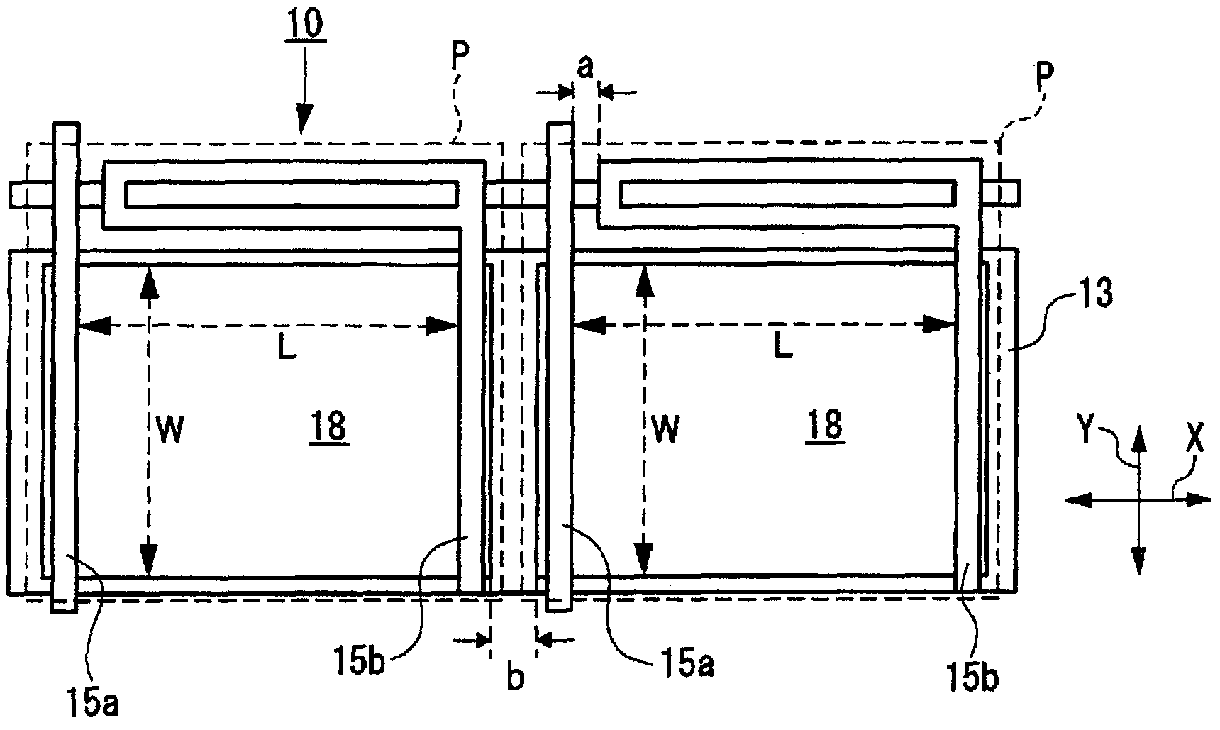
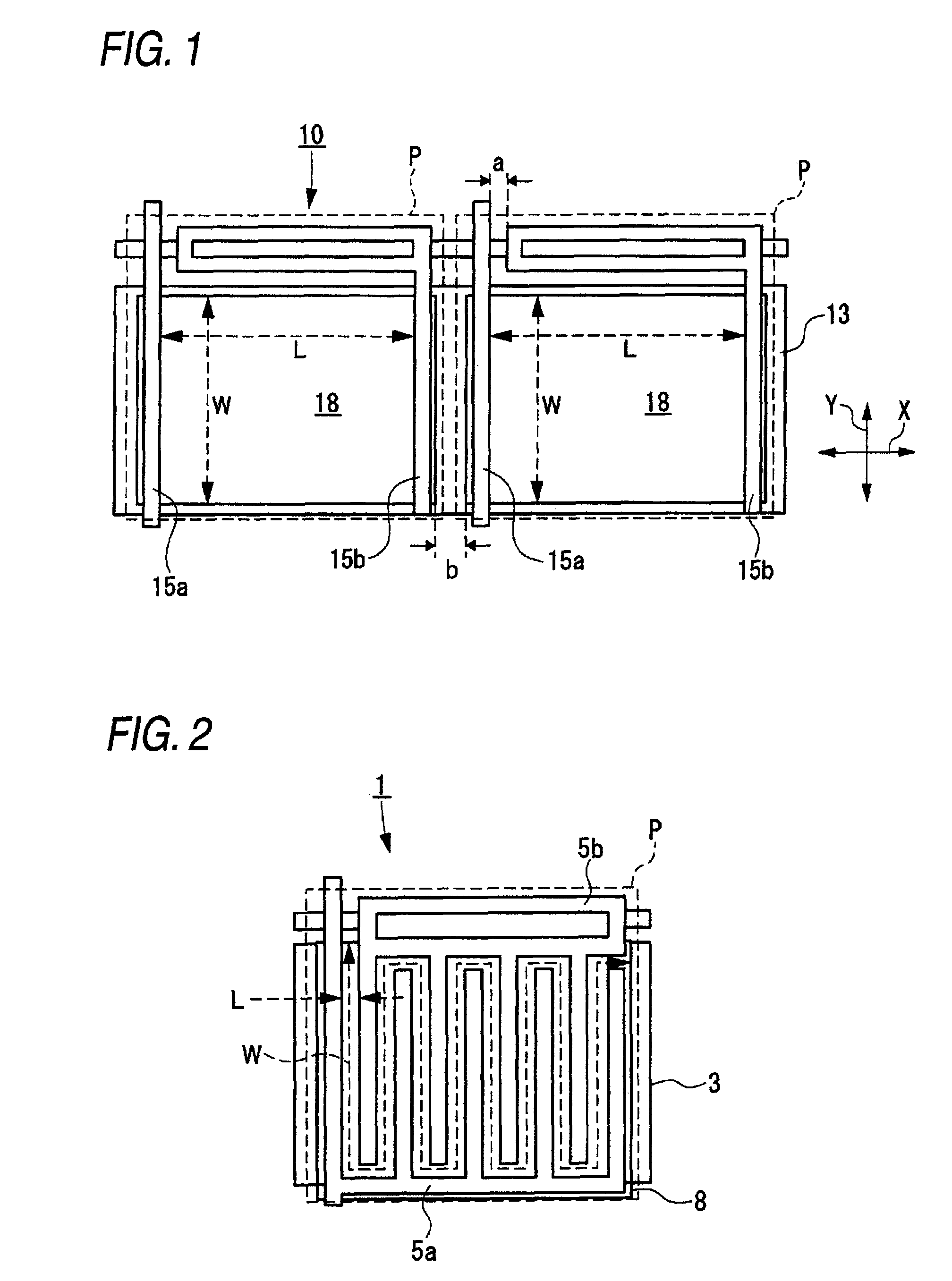
[0049]FIG. 1 is a plan view showing the configuration of a semiconductor device according to the invention. FIG. 2 is a plan view showing an example configuration of a conventional semiconductor device.

[0050]Plural pixel forming regions P are arranged in matrix form on a transparent substrate such as a glass substrate and a TFT element which is a semiconductor device 10 according to the embodiment is formed in each pixel forming region P.

[0051]A common gate electrode layer 13 is formed in pixel forming regions P on the same gate bus line among the plural pixel forming regions P arranged in matrix form. A semiconductor layer 18 is formed on the gate electrode layer 13 in each pixel forming region P. The semiconductor layer 18 is made of an inorganic oxide and patterned by printing as described later.

[0052]A source electrode layer 15a and a drain electrode layer 15b are ...


PUM


Abstract

A semiconductor device includes a substrate and a channel region which is formed above the substrate by printing, wherein a relationship L≧2a is satisfied where L is a channel length of the channel region and a is a minimum dimension among pattern dimensions and inter-pattern dimensions in the same layer as patterns that define the channel length L; and a relationship W≧2b is satisfied where W is a channel width of the channel region and b is a minimum dimension among pattern dimensions and inter-pattern dimensions in the same layer as a pattern that defines the channel width W.

Description

CROSS-REFERENCE TO RELATED APPLICATIONS[0001]This application claims the benefit of Japanese Patent Application JP 2008-098346, filed Apr. 4, 2008, the entire content of which is hereby incorporated by reference, the same as if set forth at length.FIELD OF THE INVENTION[0002]The present invention relates to a semiconductor device having a thin-film semiconductor layer and a manufacturing method of such a semiconductor device. More particularly, the invention relates to a semiconductor device suitable for light-transmission-type displays and bottom-emission-type light emission displays, a manufacturing method of such a semiconductor device, and a display device using such a semiconductor device.BACKGROUND OF THE INVENTION[0003]TFTs (thin-film transistors) are used as switching elements in active-matrix-driven panels such as LCDs (liquid crystal displays). The most common method for forming the semiconductor layer of TFTs is a method of patterning, by photolithography, an amorphous si...

Claims


Application Information

Patent Timeline
Patent Type & Authority Patents(United States)
IPC IPC(8): H01L29/10H01L21/336H01L29/786
CPCH01L27/1225H01L29/7869H01L51/0558H01L27/124H01L27/1292H01L51/0004H10K71/13H10K10/484
Inventor TANAKA, ATSUSHIUMEDA, KEN-ICHIHIGASHI, KOHEINANGU, MAKI
Owner SAMSUNG DISPLAY CO LTD
Why Eureka
Try Eureka