Method for monitoring fabrication parameter

a technology of fabrication parameters and monitoring methods, applied in the field of monitoring fabrication parameters, can solve the problems of difficult to precisely locate the tool, more difficult to further find out which fabrication parameter(s) is/are to be fixed, and the approach may not be precis

Active Publication Date: 2010-12-21
MICRON TECH INC
View PDF6 Cites 2 Cited by
  • Summary
  • Abstract
  • Description
  • Claims
  • Application Information

AI Technical Summary

Benefits of technology

[0010]The objective of the present invention is to provide a method for monitoring fabrication parameters, which effectively determines whether or not abnormality occurs in the fabrication parameters of a tool, so as to notify users in real-time for further verification or maintenance operations.
[0013]1. The present invention determines whether or not the comparing parameters are normal based on the integral difference between the variance curve of comparing parameters (fabrication parameters with unknown normality) and the variance curve of normal parameters, thereby providing a more accurate and precise determination;
[0014]2. The present invention can better determine whether or not the comparing parameters are normal by means of monitoring the variance trend of the comparing parameters.
[0015]3. The present invention is programmable and can be performed with an information product, thus providing faster execution time and achieving the effect of real-time monitoring on the comparing parameters.

Problems solved by technology

Since every step performed within a process may involve several tools, suppose an engineer is informed of an abnormality in one lot of wafers (e.g. incorrect electrical features), it is actually very difficult to precisely locate the tool causing such an error among them.
Additionally, because each tool has various fabrication parameters, it is even more challenging to further find out which fabrication parameter(s) is / are to be fixed.
However, this approach may not be precise; or sometimes the fabrication parameters have exceeded the limits, and so the tools alarmed and notified the engineer for verifications, but later it is realized that these fabrication parameters are not the actual causes for the wafer abnormality.
And more seriously, duration required for verification by engineers may result in undesirable loss of tool throughput.
As the fabrication parameters fluctuate dramatically, wafer abnormality could be accordingly generated, but conventional solutions are incapable of distinguishing variations in fabrication parameters.

Method used


Image

  • Method for monitoring fabrication parameter
  • Method for monitoring fabrication parameter
  • Method for monitoring fabrication parameter

Examples


Embodiment Construction

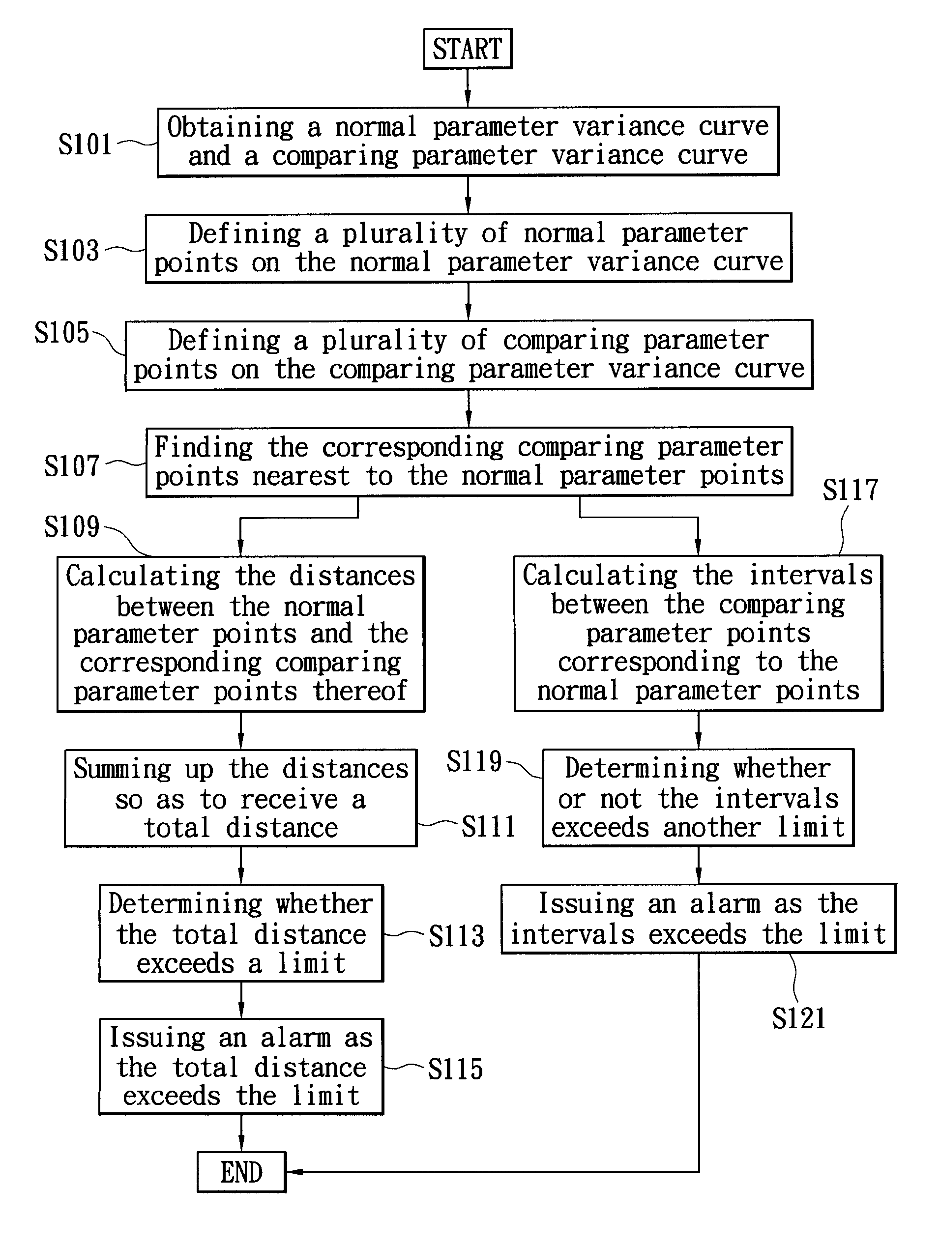
[0025]The present invention discloses a method for monitoring fabrication parameters applicable in various manufacturing workflows; herein the embodiments take semiconductor fabrications as examples.

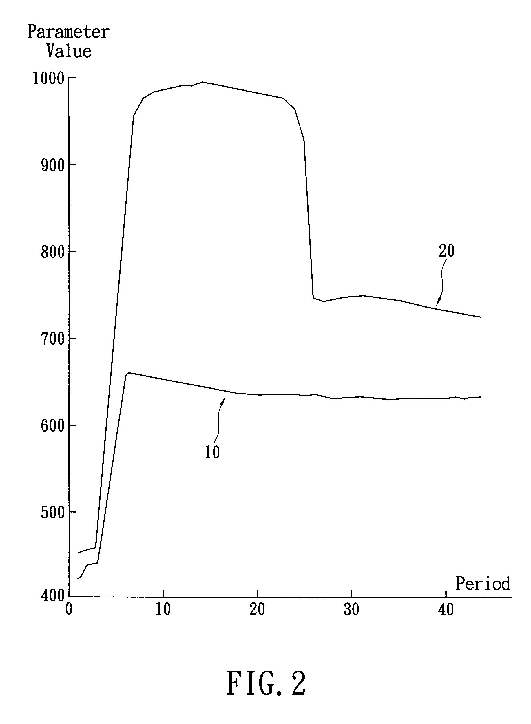
[0026]There exists several tools for semiconductor fabrication, and while the tools are machining on a lot of wafers, the fabrication parameters (e.g voltage values) of such tools may vary along the machining times; for example, a starting voltage value can be zero, then gradually increasing up to a certain value and holds, then subsequently be restored back to zero. Such a variation of fabrication parameter over time can be recorded as a parameter variance curve, and the parameter variance curve can be generated by the Fault Detection and Classification (FDC) system commonly used in the field of semiconductor.

[0027]Each fabrication parameter on a tool has its own normal parameter variance curve, and after machining on a lot of wafers by the tool, suppose the features of the wafers and d...


PUM


Abstract

A method for monitoring fabrication parameters comprises steps of: obtaining a normal parameter variance curve and a comparing parameter variance curve; defining a plurality of normal parameter points on the normal parameter variance curve; defining a plurality of comparing parameter points on the comparing parameter variance curve; finding out the corresponding comparing parameter points nearest to the normal parameter points; calculating the distances between the normal parameter points and the corresponding comparing parameter points thereof; summing up the distances so as to receive a total distance; and determining whether or not the total distance exceeds a limit. Via this arrangement, when fabrication parameter of tool is abnormal, it can be efficiently and immediately determined.

Description

BACKGROUND OF THE INVENTION[0001]1. Field of the Invention[0002]The present invention relates to a method for monitoring fabrication parameters; especially, the present invention relates to a method for monitoring fabrication parameters applicable in semiconductor manufacturing.[0003]2. Description of Related Art[0004]In semiconductor manufacturing, each lot of wafers needs to pass through various fabrication processes so as to complete and form the required semiconductor components, wherein each process may influence the final yield and throughput of the semiconductor components.[0005]Since every step performed within a process may involve several tools, suppose an engineer is informed of an abnormality in one lot of wafers (e.g. incorrect electrical features), it is actually very difficult to precisely locate the tool causing such an error among them. Additionally, because each tool has various fabrication parameters, it is even more challenging to further find out which fabricati...

Claims


Application Information

Patent Timeline
Patent Type & Authority Patents(United States)
IPC IPC(8): H01L21/00
CPCG05B19/41875H01L22/20G05B2219/31483G05B2219/32191G05B2219/45031Y02P90/02
Inventor LEE, YI FENGCHEN, CHUN CHITIAN, YUN-ZONGCHEN, WEI JUN
Owner MICRON TECH INC
Why Eureka
Try Eureka