Semiconductor memory which enables reliable data writing with low supply voltage by improving the conductance via access transistors during write operation

a technology of access transistor and data writing, which is applied in the field of single-port static random access memory, can solve the problems of inability to meet the conductance of writing operation of mos transistor pb>101/b>, inability to write operation reliable, and content stored in memory cells may become corrupted, etc., and achieve the effect of easy turning over

Inactive Publication Date: 2011-01-11
SOCIONEXT INC
View PDF8 Cites 31 Cited by
  • Summary
  • Abstract
  • Description
  • Claims
  • Application Information

AI Technical Summary

Benefits of technology

[0023]The present invention is to solve the above problem of the prior art by providing a semiconductor memory that maintains securely the contents stored in the memory cells and that enables reliable writing in the memory cells even with a low supply voltage.
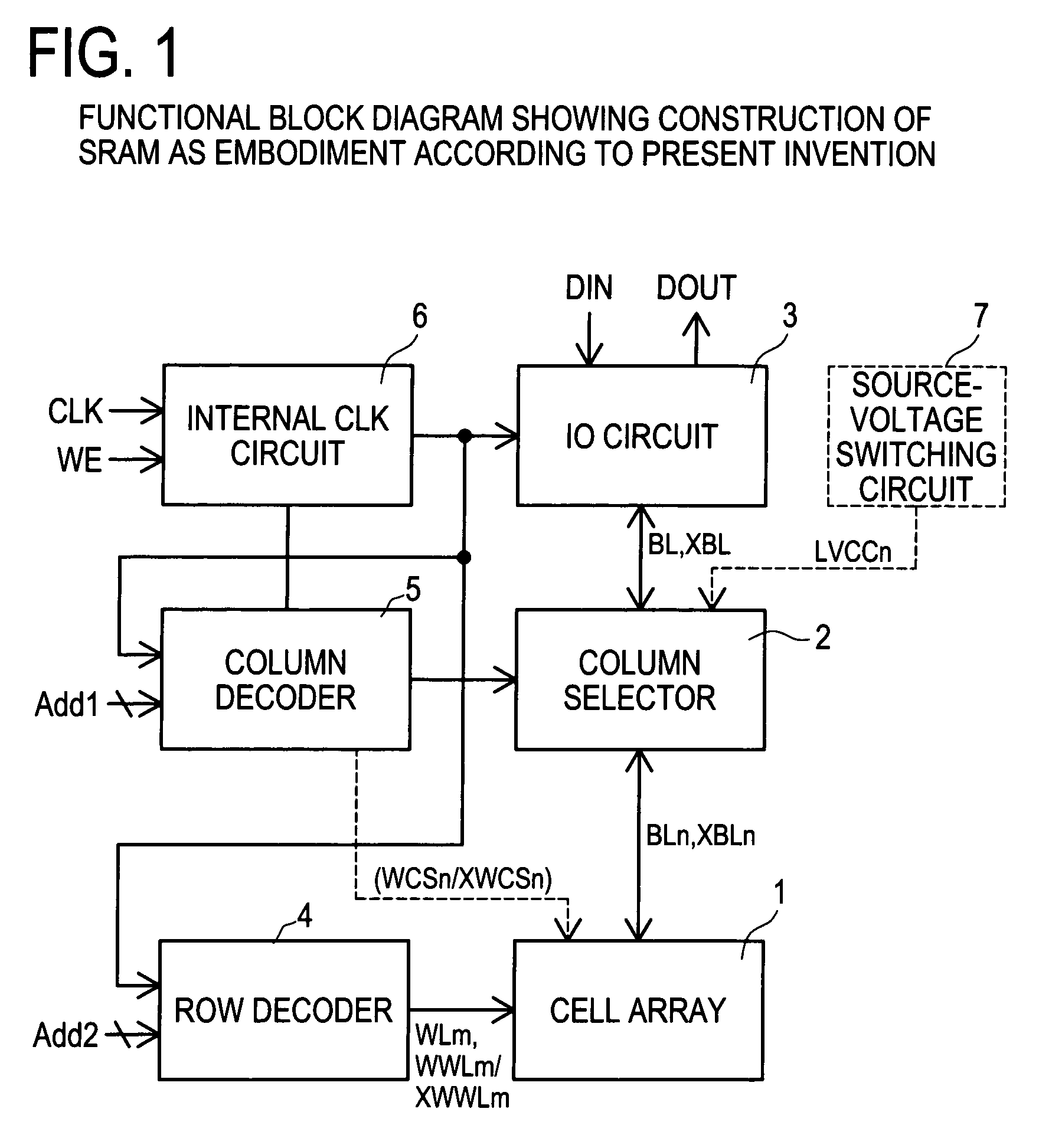
[0035]By this, for the writing operation, the conductance of the path between the bit line and the inverter is made larger than that between the output terminal of the inverter and the ground voltage. As a result, the inversion to the low level is achieved easily. For the inverter, the ratio in conductance of the transistors disposed on the supply-voltage side and on the ground-voltage side is determined to set the threshold voltage, at which the output of the inverter is turned over, to an approximately half of the supply voltage. In this way, the semiconductor memory is made reliable for maintaining the contents stored in the memory cells as well as for writing data into the memory cells.
[0046]By this, for the writing operation, the output power on the low level side or the high level side of the latch circuit, which comprises the cross-coupled inverters, becomes comparatively lower. As a result, the level on the side where the output power has decreased is easily turned over. For the inverter, the ratio in conductance of the transistors disposed on the supply-voltage side and on the ground-voltage side is determined to set the threshold voltage, at which the output of the inverter is turned over, to an approximately half of the supply voltage. In this way, the semiconductor memory is made reliable for maintaining the contents stored in the memory cells as well as for writing data into the memory cells.

Problems solved by technology

This presents a possibility that the contents stored in the memory cells may become corrupted.
However, condition n-type MOS transistor N103>p-type MOS transistor P101 in conductance for writing operation may not be satisfied because of the uneven quality of semiconductor memories as products.
If this condition is not satisfied, then it is a problem because the writing operation will not be reliable.

Method used


Image

  • Semiconductor memory which enables reliable data writing with low supply voltage by improving the conductance via access transistors during write operation
  • Semiconductor memory which enables reliable data writing with low supply voltage by improving the conductance via access transistors during write operation
  • Semiconductor memory which enables reliable data writing with low supply voltage by improving the conductance via access transistors during write operation

Examples


first embodiment

[0074]FIG. 3 is a circuit diagram showing the memory cell M00 as a The memory cell M00 comprises a p-type MOS transistor P1 and an n-type MOS transistor N1 that are connected in series between a supply voltage VCC and a ground voltage VSS, and a p-type MOS transistor P2 and an n-type MOS transistor N2 that are connected in series between a supply voltage VCC and a ground voltage VSS. These MOS transistors N1, P1, N2 and P2 constitute a pair of inverters, which are cross-coupled, and a latch circuit, which maintains electrical potentials stable at junction T1 and at junction T2.

[0075]Furthermore, the memory cell M00 comprises an n-type MOS transistor N3 and an n-type MOS transistor N5 that are disposed between bit line BL and junction T1, which leads to p-type MOS transistor P1 and n-type MOS transistor N1. It further comprises an n-type MOS transistor N4 and an n-type MOS transistor N6 that are disposed between bit line XBL and junction T2, which leads to p-type MOS transistor P2 a...

second embodiment

[0102]Therefore, the single port SRAM as a second embodiment retains the stored contents, which are represented by the electrical potentials at respective junctions T1 and T2 of the memory cell MA00, reliably even in a case where the margin for static noise on the threshold voltage Vth is relatively small because of a low supply voltage being applied. In addition, the SRAM can perform writing operation reliably.

[0103]Now, a single port SRAM as a third embodiment is explained. This SRAM has a general construction with a memory cell array similar to that of the first embodiment. The only difference is that the third embodiment comprises, instead of the write word line WWL, another write word line XWWL whose logical level is the reversal of that of the write word line WWL in the first embodiment. Therefore, only the part that relates to the write word line XWWL is explained here, so the same part as the first embodiment is not described here or is described in a simplified manner.

[0104...

third embodiment

[0112]Therefore, the single port SRAM as a third embodiment retains the stored contents, which are represented by the electrical potentials at respective junctions T1 and T2 of the memory cell MB00, reliably even in a case where the margin for static noise on the threshold voltage Vth is relatively small because of a low supply voltage being applied. In addition, the SRAM can perform writing operation reliably.

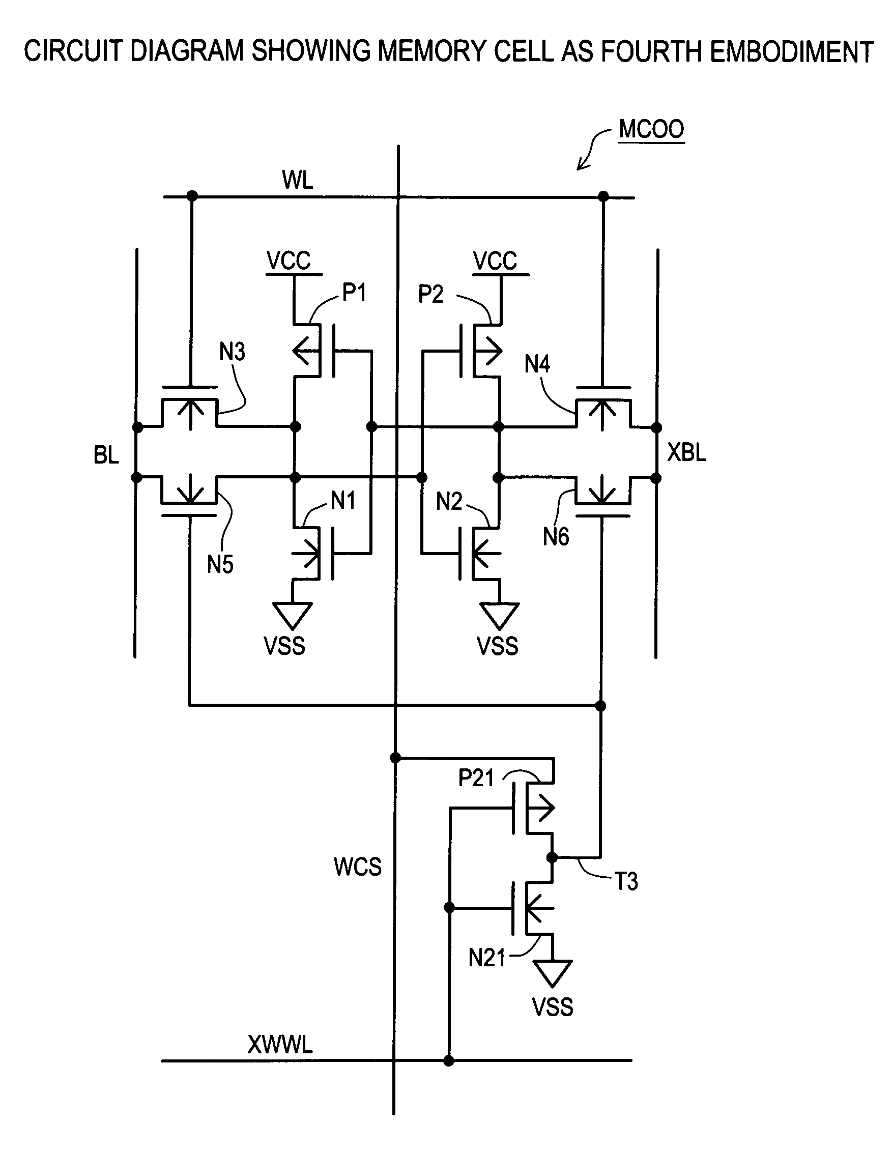
[0113]Now, a single port SRAM as a fourth embodiment is explained. This SRAM has a general construction with a memory cell array including a write word line XWWL, which is similar to that of the third embodiment. However, it is different from the third embodiment in that the memory cell array 1 includes a write column line WCS. Therefore, only the part that relates to the write column line WCS is explained, so the same part as the third embodiment is not described here or is described in a simplified manner.

[0114]At first, referring to FIG. 1, the column decoder 5 decodes lowe...


PUM


Abstract

A semiconductor memory maintains securely the stored contents in the memory cells, and it is written with data reliably even in a case where a relatively low supply voltage is applied. A memory cell M00 comprises a pair of inverters cross-coupled with each other, a first switching unit provided between bit line BL and the output terminal of one of the inverters, and a second switching unit provided between bit line XBL and the output terminal of the other inverter. The first switching unit and the second switching unit are controlled to be conductive such that the conductance of the switches be larger for the writing operation than for the reading operation.

Description

CROSS-REFERENCE TO RELATED APPLICATIONS[0001]This application is based upon and claims the benefit of priority from each of the prior Japanese Patent Application No. 2005-367150 filed on Dec. 20, 2005, the entire contents of which are incorporated herein by reference.BACKGROUND OF THE INVENTION[0002]1. Field of the Invention[0003]The present invention relates to a semiconductor memory and particularly to a single port static random-access memory (hereinafter also referred to as “SRAM” in a single word).[0004]2. Description of Related Art[0005]As an example, FIG. 14 is a circuit diagram that shows the design of a memory cell in a conventional Static Random Access Memory (SRAM).[0006]This SRAM memory cell M100 shown in FIG. 14 comprises a latch circuit that includes a p-type MOS transistor P101 and an n-type MOS transistor N101, which are connected with each other in series between a supply voltage VCC and a ground voltage VSS, and another p-type MOS transistor P102 and another n-type...

Claims


Application Information

Patent Timeline
Patent Type & Authority Patents(United States)
IPC IPC(8): G11C11/00
CPCG11C11/412
Inventor OZAWA, TAKASHI
Owner SOCIONEXT INC
Why Eureka
Try Eureka