Exposure method

a technology of exposure and method, applied in the field of exposure method, can solve problems such as unhelpful control, and achieve the effect of increasing the uniformity of a critical dimension (cd)

Active Publication Date: 2011-01-18
UNITED MICROELECTRONICS CORP
View PDF8 Cites 8 Cited by
  • Summary
  • Abstract
  • Description
  • Claims
  • Application Information

AI Technical Summary

Benefits of technology

[0007]The present invention is directed to an exposure method which can increase uniformity of a critical dimension (CD) on a shot-to-shot level.
[0008]The present invention provides an exposure method capable of improving the overlay alignment of successive material layers in each exposure region.
[0017]In the process for forming the device on the wafer, while the exposure process is performed on each of the exposure regions on the wafer, the exposure process parameter set of the exposure tool is adjusted according to exposure-region feedback parameter sets, which are corresponding to the exposure regions respectively, in the feedback parameter map, which is corresponding to the tool path to be used and the device to be formed, and thereby the shot-by-shot exposure parameter feedback adjustment is performed in each of the exposure regions on a single wafer according to the exposure-region feedback parameter set corresponding to the exposure region. Therefore, the uniformity of the critical dimension on the shot-to-shot level in the single wafer is improved and the overlay alignment between the successive material layers in each exposure region is improved as well.

Problems solved by technology

However, the conventional automatic feedback system only provides a fixed feedback value for every wafer in every lot, which is not helpful in controlling the variations of the CDs among every exposure region on the wafer.

Method used


Image

  • Exposure method
  • Exposure method
  • Exposure method

Examples


Embodiment Construction

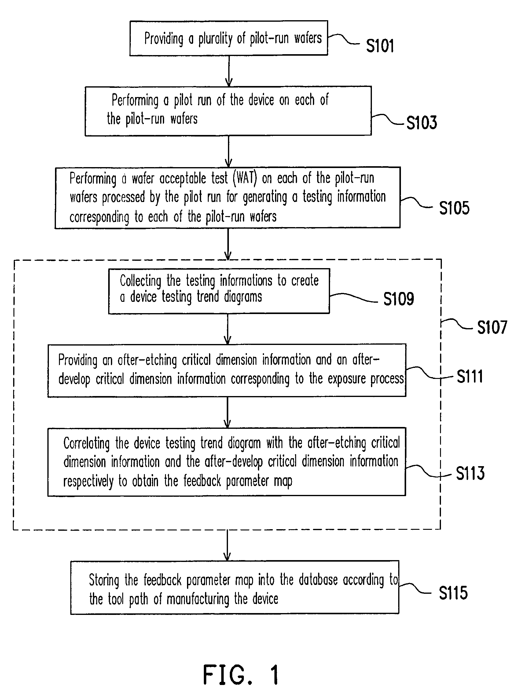
[0022]FIG. 1 illustrates a processing flow of forming a feedback parameter map according to the present invention. Referring to FIG. 1, a plurality of pilot-run wafers is provided in step S101. A quantity of the pilot-run wafers can be that of wafers in a lot, such as 25 pieces. After that, a pilot-run process for manufacturing a device is performed on each of the pilot-run wafers through a tool path in step S103. The device can be as small as a simple circuit device or as big as a product having a complicated circuit layout. Furthermore, the tool path is a path in which various machines required to be used in the processing flow for manufacturing the device are arranged in order according to the operating sequence of manufacturing the aforesaid device. Thereafter, in step S105, a wafer acceptable test (WAT) is performed on each of the pilot-run wafers undergone the pilot-run process to generate various testing information. Each testing information is corresponding to one of the pil...


PUM

PropertyMeasurementUnit
critical dimensionaaaaaaaaaa
light incident angleaaaaaaaaaa
thresholdaaaaaaaaaa

Abstract

The invention provides an exposure method for manufacturing a device. The method includes providing a wafer having several exposure regions with a photoresist layer covering thereon. A feedback parameter map with several exposure-region feedback parameter sets respectively corresponds to the exposure regions of the wafer. At least one of the exposure-region feedback parameter sets is different from the rest of the exposure-region feedback parameter sets. According to the feedback parameter map, an exposure process is sequentially performed on each of the exposure regions of the wafer through an exposure tool to pattern the photoresist layer on the wafer. While the exposure tool performs the exposure process on each of the exposure regions, an exposure process parameter set of the exposure tool is adjusted based on the exposure-region feedback parameter sets corresponding to the exposure region in the feedback parameter map.

Description

BACKGROUND OF THE INVENTION[0001]1. Field of the Invention[0002]The present invention relates to an exposure method, and in particular, to an exposure method for increasing uniformity of a critical dimension on a shot-to-shot level on the same wafer in a wafer acceptable test (WAT) step.[0003]2. Description of Related Art[0004]In a manufacturing process of an integrated circuit, a photolithography process is used to transfer customized circuit patterns on a photo mask to thin films formed on a wafer. An image transferring process includes forming a photoresist layer on a non-process layer. Then, the photoresist layer is illuminated through a photo mask having the customized circuit patterns. After that, a developing process is performed on the photoresist layer. Thereafter, an etching process is performed on the non-process layer by using a patterned photoresist layer as a mask. Hence, the image transferring process is accomplished.[0005]Generally, one of basic parameters affecting ...

Claims


Application Information

Patent Timeline
Patent Type & Authority Patents(United States)
IPC IPC(8): G03F9/00G03C5/00
CPCG03F7/70525G03F7/70625G03F7/70633
Inventor CHEN, JU-TEWU, WEN-TSUNG
Owner UNITED MICROELECTRONICS CORP
Why Eureka
Try Eureka