Stacked mounting structure

a mounting structure and stacked technology, applied in the direction of stacked spaced pcbs, printed circuit aspects, electrical apparatus construction details, etc., can solve the problems of increased contact resistance, reduced productivity, and difficulty in connecting the terminals

Active Publication Date: 2011-01-25
OLYMPUS CORP
View PDF6 Cites 30 Cited by
  • Summary
  • Abstract
  • Description
  • Claims
  • Application Information

AI Technical Summary

Problems solved by technology

However, when the terminals are formed by the ink-jet method such that the terminals are not protruded with respect to the side surface of the semiconductor chip, it is difficult to connect the terminals assuredly.
Moreover, there is a problem that a contact resistance is increased.
When the terminals 3 are drawn up to the side surface of the semiconductor chip 1 in such manner, it results in a decrease in productivity.
Therefore, there is an increase in a size of the stacked mounting structure.

Method used


Image

  • Stacked mounting structure
  • Stacked mounting structure
  • Stacked mounting structure

Examples


first embodiment

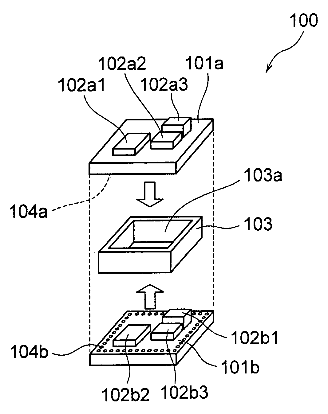
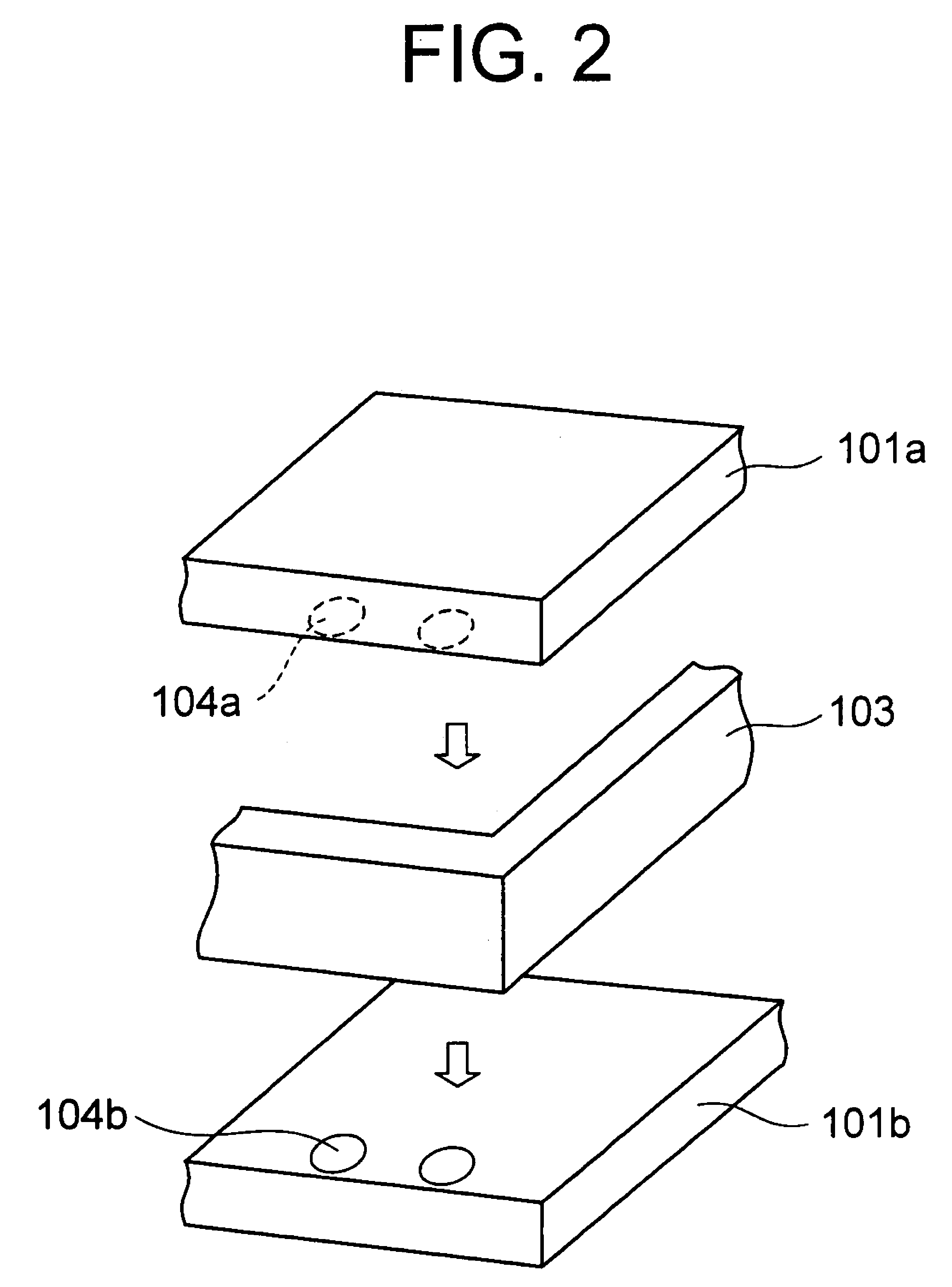
[0068]FIG. 1 shows a perspective view of a state in which a stacked mounting structure 100 according to a first embodiment of the present invention is disassembled. Various devices 102a1, 102a2, and 102a3 (hereinafter called as “devices 102a1 etc.”) which are electronic components including active components and passive components are mounted on a first substrate 101a. Moreover, various other devices 102b1, 102b2, and 102b3 (hereinafter called as “devices 102b1 etc.”) which are electronic components including active components and passive components are mounted on a second substrate 101b. The first substrate 101a and the second substrate 101b are disposed to be facing mutually. The first substrate 101a corresponds to a first member. The second substrate 101b corresponds to a second substrate.

[0069]Each of the first substrate 101a, the second substrate 101b, and an intermediate substrate 103 which will be described later, is formed of a material such as an organic substrate, a cerami...

second embodiment

[0092]Next, a stacked mounting structure 200 according to a second embodiment of the present invention will be described below. Same reference numerals are assigned to components which are same as in the first embodiment, and description to be repeated is omitted. FIG. 7 shows upon enlarging a structure near the intermediate substrate 103. Moreover, FIG. 8 shows a perspective view of the stacked mounting structure 200.

[0093]As shown in FIG. 7, in the second embodiment, a concave portion 106 is formed on the side surface of the intermediate substrate 103. Accordingly, the structure is such that the first connecting terminal104a of the first substrate 101a and the second connecting terminal 104b of the second substrate 101b are exposed. The concave portion 106, as shown in FIG. 8, is formed spreading over a periphery of the intermediate substrate 103. Moreover, the concave portion 106 is formed continuously with a constant depth.

[0094]According to the second embodiment, the concave po...

third embodiment

[0101]Next, a stacked mounting structure 120 according to a third embodiment of the present invention will be described below. Same reference numerals are assigned to the components same as in the embodiments described above, and the description to be repeated is omitted.

[0102]FIG. 11 shows a schematic structure of the stacked mounting structure 120. The concave portion 106 formed in the intermediate substrate 103 includes a first concave portion 106a near the first substrate 101a and a second concave portion 106b near the second substrate 101b.

[0103]In this manner, the concave portion 106 formed in the intermediate substrate 103 is a groove structure with one end of the groove reaching the first substrate 101a (not shown in FIG. 11) and the other end of the groove reaching the second substrate 101b. Moreover, the structure is such that each of the first connecting terminal 104a (not shown in FIG. 11) of the first substrate 101a and the second connecting terminal 104b of the second...


PUM

PropertyMeasurementUnit
electroconductiveaaaaaaaaaa
groove depthaaaaaaaaaa
thicknessaaaaaaaaaa

Abstract

A stacked mounting structure includes a first substrate, a second substrate, and an intermediate substrate which has a space accommodating therein components to be mounted. A first contact (connecting) terminal and a second contact (connecting) terminal are formed on the first substrate and the second substrate, and have a wire which is formed on a side surface of the intermediate substrate. By formation of the intermediate substrate to be on an inner side than an edge surface of the substrates, a part of the two contact terminals respectively are exposed. One end of the wire is connected to an exposed portion of the first contact terminal, and the other end of the wire is connected to an exposed portion of the second contact terminal.

Description

CROSS-REFERENCE TO RELATED APPLICATION[0001]The present application is based upon and claims the benefit of priority from the prior Japanese Patent Application Nos. 2006-125078 filed on Apr. 28, 2006 and 2007-25367 filed on Feb. 5, 2007; the entire contents of which are incorporated herein by referenceBACKGROUND OF THE INVENTION[0002]1. Field of the Invention[0003]The present invention relates to a stacked mounting structure, and particularly to a three-dimensional stacked mounting structure which is made by stacking a plurality of members in a direction of thickness of the members, and a method of manufacturing the stacked mounting structure.[0004]2. Description of the Related Art[0005]A technology related to a manufacturing method of a three-dimensional mounting module which includes a process of connecting semiconductor chips by stacking has hitherto been proposed (refer to Japanese Patent Application Laid-open Publication No. 2004-303884 for example). In the conventional technol...

Claims


Application Information

Patent Timeline
Patent Type & Authority Patents(United States)
CPCH05K1/144H05K3/3442H05K3/403H05K3/4685H05K2201/042H01L2224/16H05K2201/09181H05K2201/10378H05K2201/2018Y10T29/49126H05K2201/09154
Inventor MOTOHARA, HIROYUKIKONDOH, YOUNAKAMURA, MIKIOSEKIDO, TAKANORIYASUNAGA, SHINJI
Owner OLYMPUS CORP
Why Eureka
Try Eureka