Composite connection structure and method of manufacturing

a technology of composite connection and manufacturing method, which is applied in the direction of manufacturing tools, sustainable manufacturing/processing, and final product manufacturing, etc., can solve the problems of lead containing solder waste treatment, lead contamination, and high cost of lead removal for cleaning up of solder from metal masks, and the connection structure has been largely restricted

Inactive Publication Date: 2002-01-08
TEXAS INSTR INC
View PDF3 Cites 172 Cited by
  • Summary
  • Abstract
  • Description
  • Claims
  • Application Information

AI Technical Summary

Problems solved by technology

Owing to manufacturing difficulty in handling and placement of the balls, this procedure was replaced by forming solder connection structures or bumps on the chip terminals while still in wafer form.
Owing to the short, rigid connecting structures, fatigue at the solder joints is a concern.
Waste treatment for clean-up of lead containing solder from said metal masks is both expensive and a growing environmental issue.
However, the connecting structures have been largely restricted to the use of lead / tin solders of different compositions which are subject to fatigue failures as a function of thermally induced stresses.
Further, lead (Pb) containing solders on the surface of soft error sensitive devices has caused concern due to alpha particle emission from lead (Pb), as well as environmental issues with the use of lead (Pb).
The reliability concerns are somewhat similar to those for flip-chip in that thermally induced stresses in the solder joints result from mismatches CTE and Young's modulus and which may vary within the package and board area due to the large size and underlying construction.
Package weight can contribute to the difficulty in controlling stand off distance of solder bumped packages.
As with BGA and flip-chip, the presence of leaded compounds presents an environmental issue to some users.
Clean-up of fluxes presents reliability concerns with the small stand-off height of CSP.
This process of fabricating polymeric bumps is extremely expensive, is limited by processing capabilities and in some cases will not be compatible with thermal testing routinely required of integrated circuits.
The fabrication process is not unlike that described above for polymeric bumps and is expensive.

Method used


Image

  • Composite connection structure and method of manufacturing
  • Composite connection structure and method of manufacturing
  • Composite connection structure and method of manufacturing

Examples


Embodiment Construction

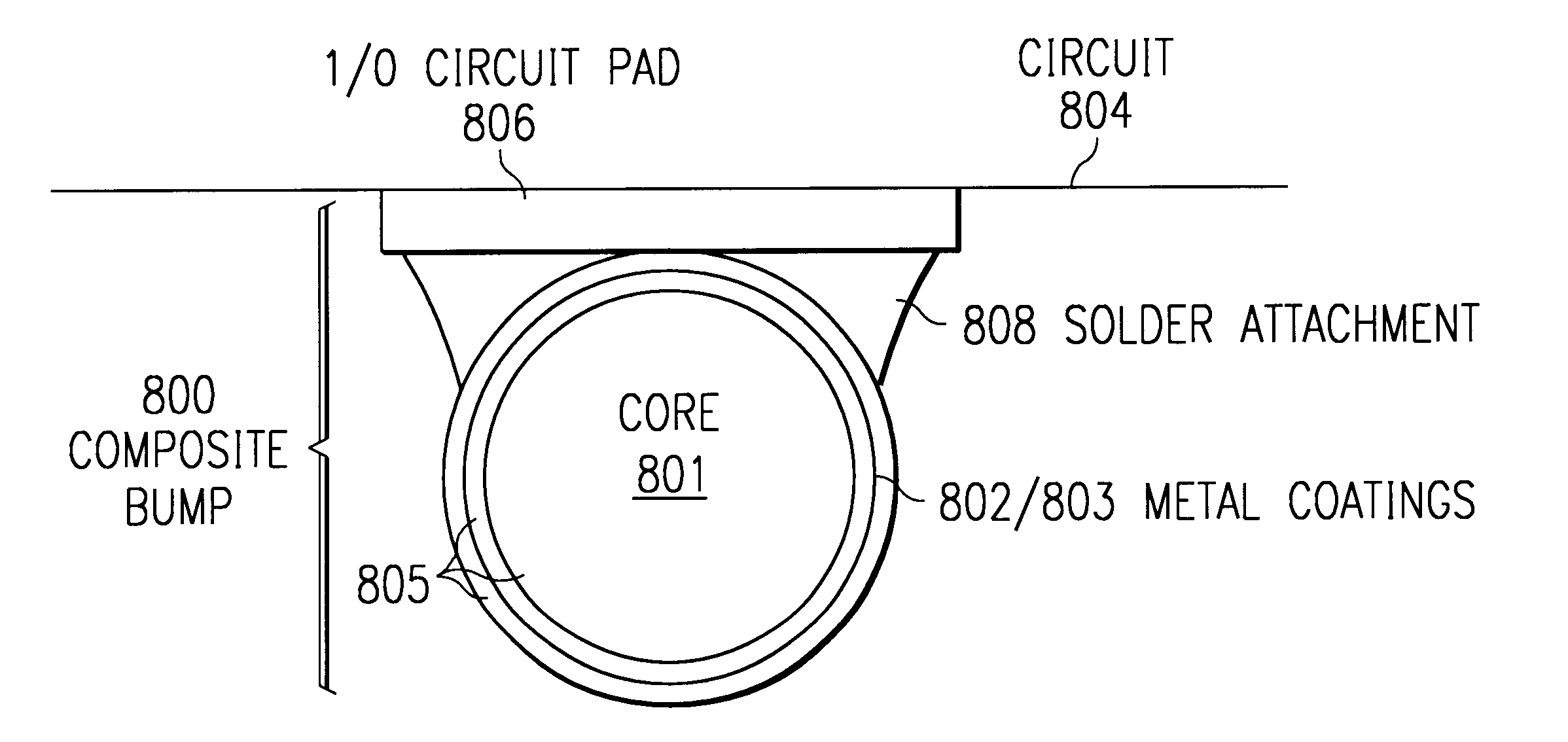
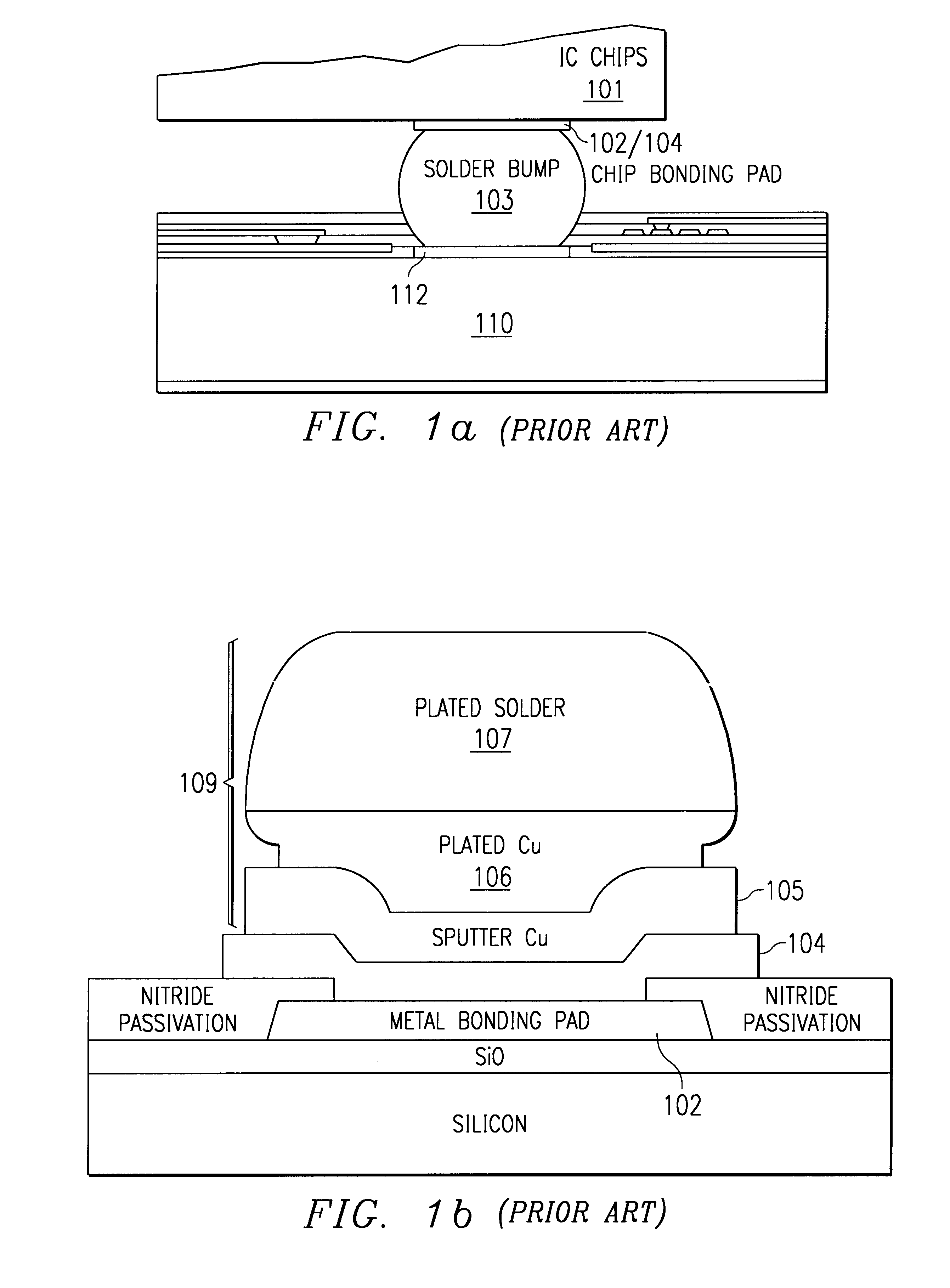
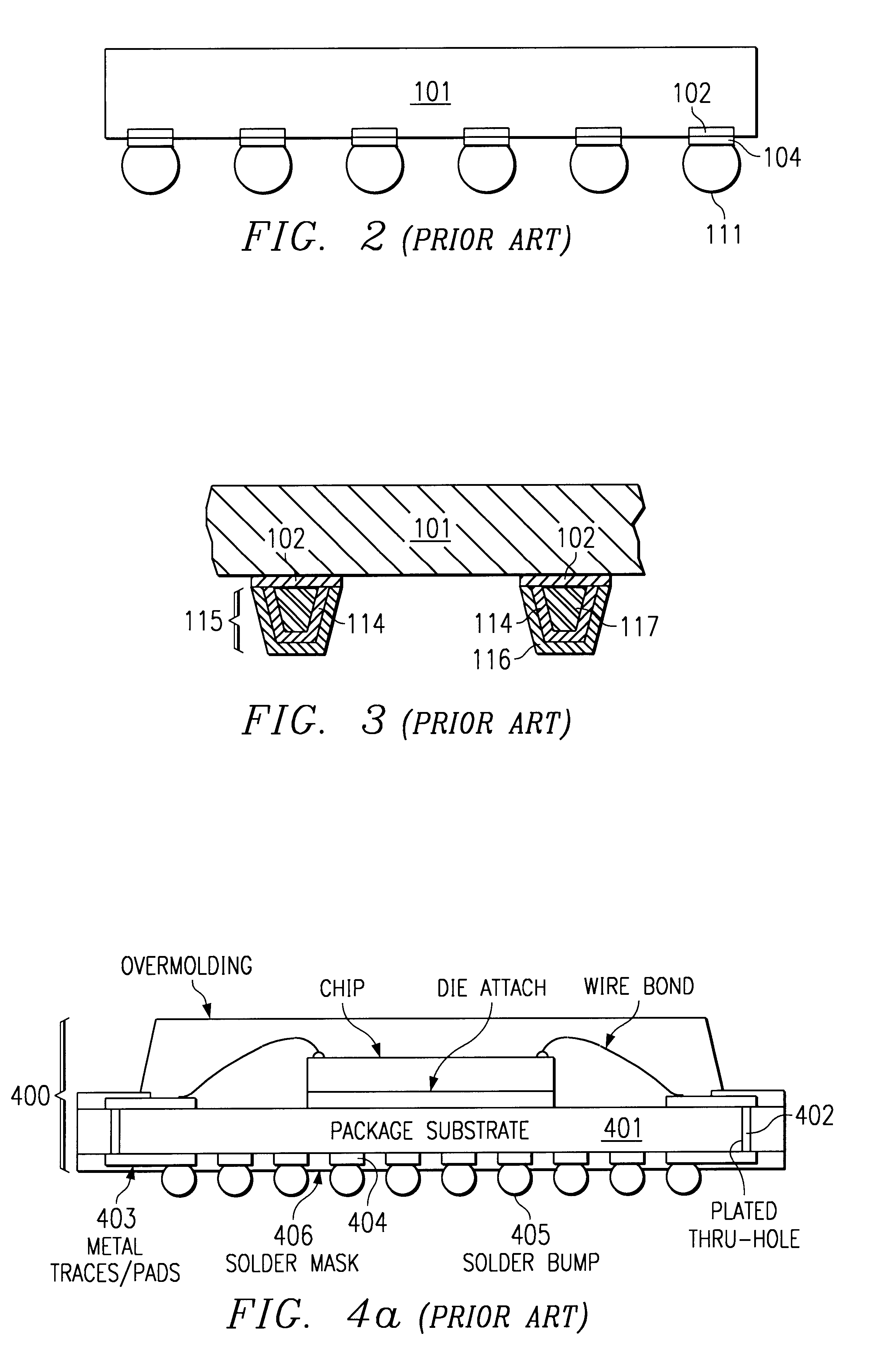
Turning now to the drawings, in FIG. 1a there is shown an example of a flip-chip connection structure as disclosed in prior art which includes an integrated circuit 101, with contact pads 102, and a solder bump connecting structure 103. The solder bump is further connected to a substrate 110 with contact pads 112. FIG. 1b depicts in greater detail the composition of a given flip-chip bump structure 109. In this construction, bump structures are fabricated on the input / output contact pads 102 of all chips on an integrated circuit wafer (which is not shown). Said structures are fabricated by a series of metal deposition steps which include sputtering and patterning the under bump (UBM) metallization 104 which protects the thin film aluminum bond pad 102. This is followed by sputtering a seed layer of copper 105 which will be used as the contact electrode for electroplating thicker layers of copper 106 and solder 107 which in turn form the bulk of the bump structure 109. A photoresist ...


PUM

PropertyMeasurementUnit
thicknessaaaaaaaaaa
diameteraaaaaaaaaa
diameteraaaaaaaaaa

Abstract

A bump connection structure and a method of attachment to integrated circuits or packages is provided which comprises a prefabricated core structure coated with solderable metal layers to form a composite bump. Said composite bump is aligned to contact pads of the chip or package which have been coated with solder paste, and the assembly heated to form a metallurgical bond. The prefabricated core structures are comprised of metal, plastic or ceramic of the size and dictated by package standards. The connection structure is preferably lead free.

Description

This invention relates generally to the field of integrated circuit interconnections, and more particularly to a bumped connection structure used on integrated circuits, and on other assemblies, such as integrated circuit packages.BRIEF DESCRIPTION OF PRIOR ARTA number of forces have influenced the selection o structures which provide connection of an integrateded circuit to the next level of interconnection. Lead density has been a major factor in focusing designers toward connections which are contained within the area of the integrated circuit or of first level packaging, such as flip-chip, ball grid array (BGA) and chip size packages (CSP). These interconnections are generally referred to as area array interconnections and are formed by a bump type of structure as opposed to a flexible lead type of structure which extends out from the perimeter of the integrated circuit element.Connections for these assemblies are designed as a finely pitched matrix of conductive contacts on the...

Claims


Application Information

Patent Timeline
Patent Type & Authority Patents(United States)
IPC IPC(8): H01L23/498H01L23/48H05K3/34H01L23/485
CPCH01L23/49816H01L24/12H01L27/14618H01L27/14636H05K3/3436H01L2224/11334H01L2224/13099H01L2224/16H01L2224/48091H01L2224/48227H01L2224/73265H01L2225/0651H01L2225/06513H01L2225/06517H01L2225/06586H01L2924/01013H01L2924/01022H01L2924/01029H01L2924/01042H01L2924/01046H01L2924/01051H01L2924/01074H01L2924/01078H01L2924/01079H01L2924/01082H01L2924/01322H01L2924/09701H01L2924/14H01L2924/15311H01L2924/16152H01L2924/30107H05K3/3463H05K2201/0212H05K2201/10234H05K2203/047H01L24/11H01L2924/10253H01L2224/32225H01L2924/014H01L2924/01047H01L2924/01033H01L2924/01024H01L2924/01006H01L2924/01005H01L24/48H01L2924/00014H01L2924/00H01L2224/02377H01L2224/05599H01L2224/45099H01L2224/85399H01L2924/15787H01L2924/181Y02P70/50H01L2224/45015H01L2924/207H01L2924/00012
Inventor ABBOTT, DONALD C.ROMM, DOUGLAS W.
Owner TEXAS INSTR INC
Why Eureka
Try Eureka