Chip package with multiple chips connected by bumps

a chip and bump technology, applied in the field of chip assembling, can solve the problems of reducing the yield of the package, difficult fabrication process, etc., and achieve the effect of improving the reliability of assembling

Inactive Publication Date: 2007-07-10
QUALCOMM INC
View PDF22 Cites 176 Cited by
  • Summary
  • Abstract
  • Description
  • Claims
  • Application Information

AI Technical Summary

Benefits of technology

[0012]The present invention provides a method of assembling chips with greatly enhanced assemble reliability.

Problems solved by technology

However, there is some difficulty in the fabrication process thereof.
A short circuit is thus caused to reduce the package yield.

Method used


Image

  • Chip package with multiple chips connected by bumps
  • Chip package with multiple chips connected by bumps
  • Chip package with multiple chips connected by bumps

Examples


first embodiment

[0041]Referring to FIGS. 6 and 7, a cross sectional schematic view of a method for assembling carriers according to the present invention is shown. As shown in FIG. 6, two carriers 210, 220, that is, the first and second carriers 210 and 220 are provided. The first carrier 210 has multiple terminals 212 exposed at a surface thereof. The second carrier 220 has multiple terminals 222 exposed at a surface thereof. The first and second carrier 210 and 220 each includes a chip, a substrate or a ceramic substrate.

[0042]Multiple conductive pillars 230 are formed on the terminals 212 of the first carrier 210, while a conductive connecting material 240 is formed on each of the terminals 222 of the second carrier 220. The material of the conductive pillars 230 is selected from tin, lead, copper, gold, silver, zinc, bismuth, magnesium, antimony, indium and an alloy thereof. The conductive connecting material 240 is in a paste form and can be formed by mixing metal particles and a flux. The con...

sixth embodiment

[0050]Referring to FIGS. 13 and 14, the method of assembling carriers in the present invention is illustrated. Those denoted by the same reference numerals in FIG. 1 indicate the same devices or members and are not described again. After providing the first and second carriers 210 and 220, conductive pillars 230 are formed on each terminal 212 of the first carrier 210. The material of the conductive pillar 230 includes tin, lead, copper, gold, silver, zinc, bismuth, magnesium, antimony, indium or an alloy of the above materials. Conductive pillars 262 and a conductive connecting material 264 are further formed on each terminal 222 of the second carrier 220. The conductive pillars 262 are located on each terminal 222, while the conductive connecting material 264 is formed on the conductive pillars 262 and has a bottom surface 266 in contact with the conductive pillars 262. The materials of the conductive pillars 262 and the conductive connecting material 264 includes tin, lead, coppe...

fourth embodiment

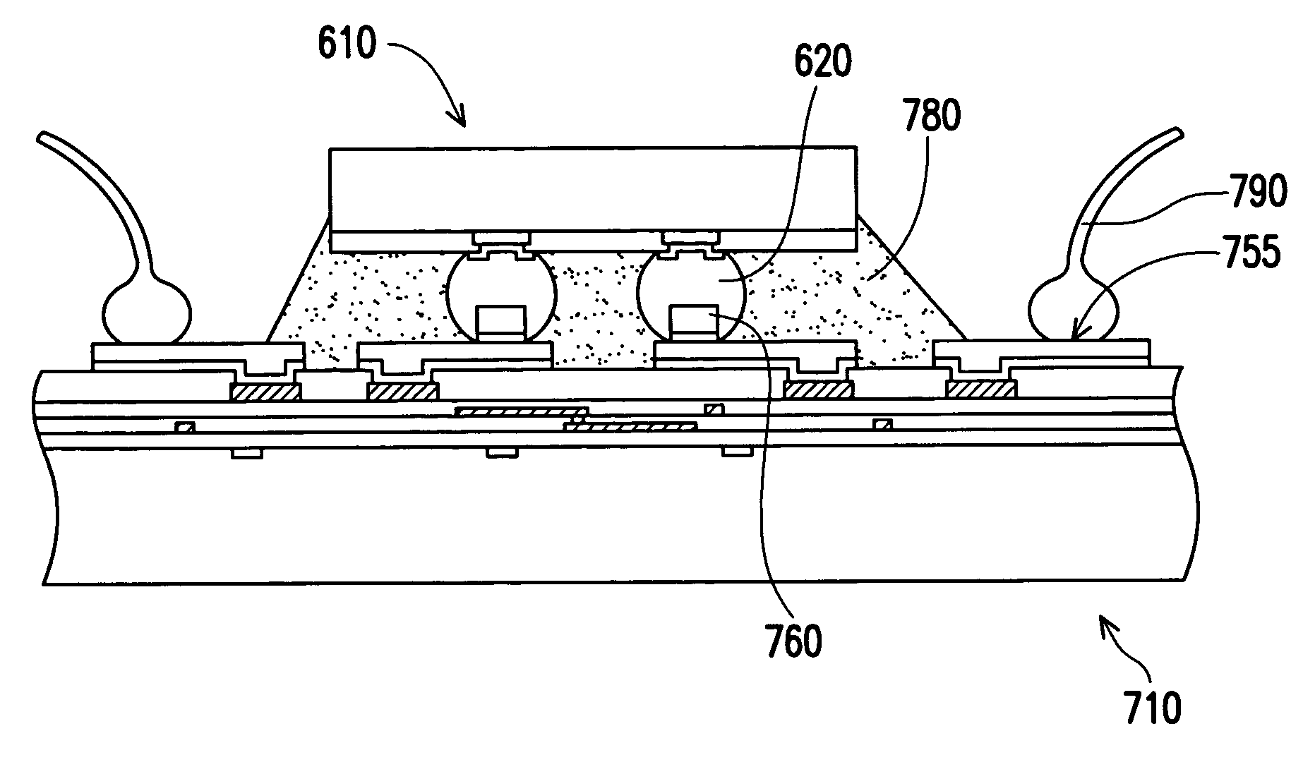
[0072]In the above embodiments, the conductive pillar and the conductive connecting material are used to electrically connect the first chip and the carrier. However, the present invention is not limited to such electric connection. Other method such as wire bonding can also be used for electrically connecting the first chip and the carrier as shown in FIGS. 37 to 42, which illustrate the cross sectional view of the multi-chip package module fabrication in the present invention.

[0073]In FIG. 37, a first chip 410 and a second chip 420 are provided. The first chip 410 has an active surface 414 and a rear surface 416 opposing to the active surface 414. The first chip 410 has a plurality of terminals 412 formed on the active surface 414. A plurality of conductive pillars 430 is formed on the terminals 412 of the active surface 414 of the first chip 410. A conductive connecting material 432 is formed on the conductive pillars 430. The method for forming the conductive pillars 430 and the...


PUM


Abstract

A method of assembling chips. A first chip and a second chip are provided. At least one conductive pillar is formed on the first chip, and a conductive connecting material is formed on the conductive pillar. The second chip also comprises at least one conductive pillar. The first chip is connected to the second chip via the conductive pillars and the conductive connecting material.

Description

CROSS-REFERENCE TO RELATED APPLICATION[0001]This application claims the priority benefit of Taiwan application serial no. 91125126, filed on Oct. 25, 2002. This application is related to application Ser. No. 09 / 798,654 flied on Mar. 5, 2001, now U.S. Pat. No. 6,818,545; and related to application Ser. No. 10 / 935,451 filed on Sep. 7, 2004, now pending; and related to application Ser. No. 09 / 953,525 filed on Sep. 17, 2001, now U.S. Pat. No. 6,642,136; and related to application Ser. No. 10 / 638,454 filed on Aug. 11, 2003, now Pat. No. 6,917,119; and related to application Ser. No. 11 / 120,234 tiled on May 2, 2005, now pending; and related to application Ser. No. 09 / 837,007 filed on Apr. 18, 2001, now pending; and related to application Ser. No. 10 / 055,580 filed on Jan. 22, 2002, now pending; and related to application Ser. No. 10 / 174,357 filed on Jun. 17, 2002, now U.S. Pat. No. 6,784,087; and related to application Ser. No. 10 / 874,704 filed on Oct. 27, 2003, now pending; and related to...

Claims


Application Information

Patent Timeline
Patent Type & Authority Patents(United States)
IPC IPC(8): H01L29/40H01L23/48H01L23/52H05K3/24H05K3/32H01L21/60H01L21/68H01L21/98H01L23/485H01L25/065
CPCH01L21/568H01L21/6835H01L24/03H01L24/05H01L24/11H01L24/12H01L24/16H01L24/48H01L24/73H01L24/81H01L25/0657H01L25/50H01L2924/15311H01L2224/13109H01L2224/32145H01L2224/32225H01L2224/73204H01L2924/00013H01L2924/00014H01L2924/01024H01L2924/01033H01L2224/81011H01L2224/81191H01L2224/32245H01L2224/16225H01L2924/15151H01L2924/0002H01L2224/0401H01L2224/04042H01L2224/05568H01L2224/05599H01L2224/1132H01L2224/1147H01L2224/13111H01L2224/13139H01L2224/13144H01L2224/13147H01L2224/13609H01L2224/16145H01L2224/48091H01L2224/48227H01L2224/48247H01L2224/48465H01L2224/731H01L2224/73207H01L2224/73265H01L2224/81193H01L2224/8121H01L2224/81815H01L2224/83102H01L2224/85399H01L2224/92125H01L2225/0651H01L2225/06513H01L2225/06527H01L2924/01005H01L2924/01006H01L2924/01007H01L2924/01012H01L2924/01013H01L2924/01014H01L2924/01022H01L2924/01028H01L2924/01029H01L2924/0103H01L2924/01047H01L2924/01049H01L2924/0105H01L2924/01051H01L2924/01073H01L2924/01074H01L2924/01079H01L2924/01082H01L2924/01083H01L2924/014H01L2924/04941H01L2924/04953H01L2924/05042H01L2924/09701H01L2224/13099H01L2224/45099H01L2924/00H01L2224/05552H01L2924/15787H01L2924/181H01L2224/81024H01L2224/8191H01L2224/02166H01L2924/00012
Inventor LIN, SHIH-HSIUNGLIN, MOU-SHIUNG
Owner QUALCOMM INC
Why Eureka
Try Eureka