

Probe card assembly and kit, and methods of using same
a technology of probe card and assembly, which is applied in the direction of printed circuit assembling, non-electric welding apparatus, printed element electric connection formation, etc., can solve the problems of dies being "good" (full functional), dies being "bad" (non functional), and certain difficulties inherent in any technique for probing semiconductor dies, so as to achieve convenient control of impedance, easy demountability, and effective shielding
- Summary
- Abstract
- Description
- Claims
- Application Information
AI Technical Summary
Benefits of technology
Problems solved by technology
Method used
Image

Examples
Embodiment Construction
#1
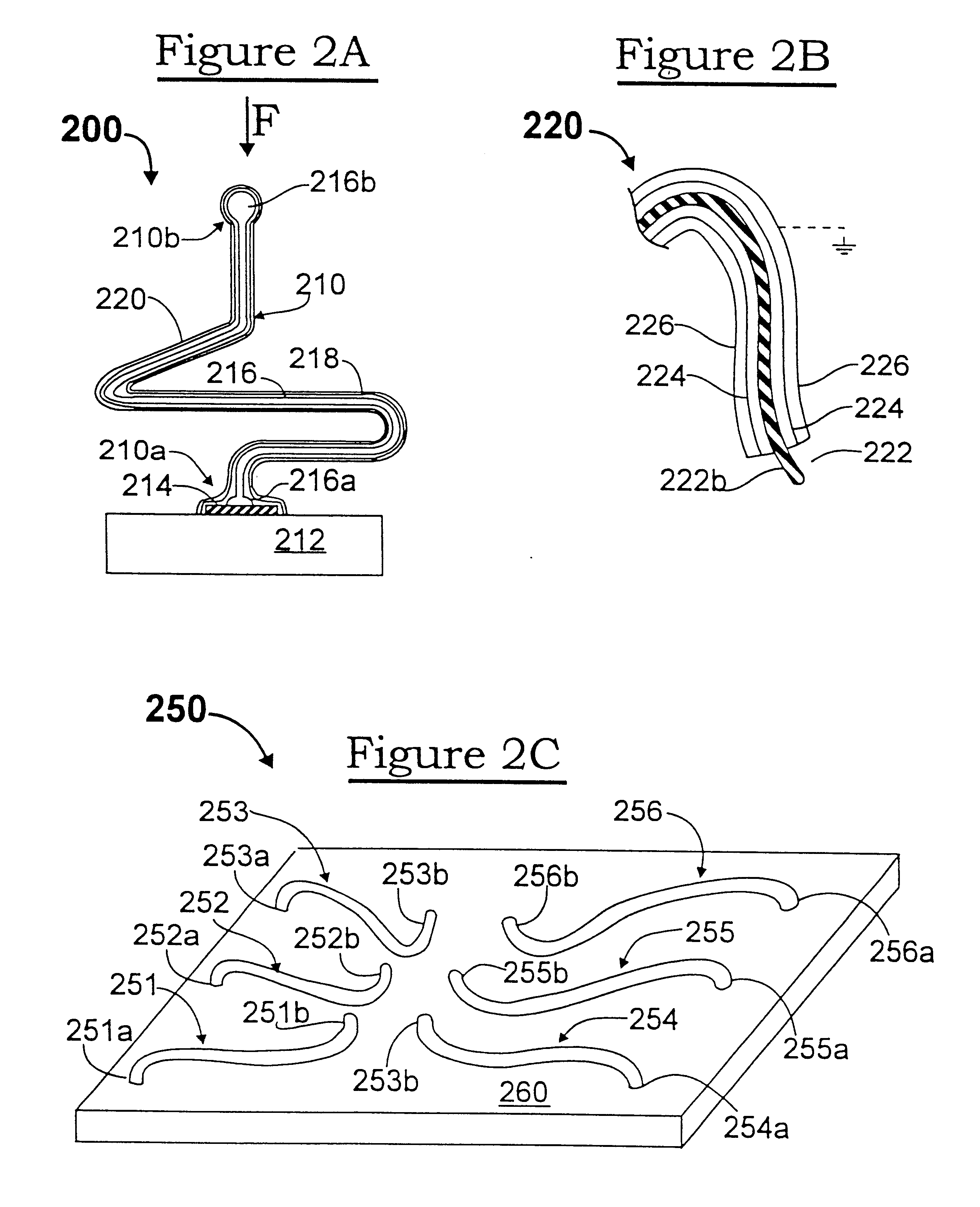
FIG. 3A illustrates an embodiment 300 of an interposer, using the interconnection elements of the invention. Generally, an insulating substrate 302, such as a PCB-type substrate, is provided with a plurality (two of many shown) of electrically conductive through holes (e.g., plated vias) 306, 308, or the like, each having conductive portions exposed on the top (upper) 302a and bottom (lower) 302b surfaces of the insulating substrate 302.
A pair of soft cores 311 and 312 are attached to the exposed portion of the through hole 306 on the top surface 302a of the substrate 302. A pair of soft cores 313 and 314 are attached to the exposed portion of the through hole 306 on the bottom surface of the substrate 302. Similarly, a pair of soft cores 315 and 316 are attached to the exposed portion of the through hole 308 on the top surface of the substrate 302, and a pair of soft cores 317 and 318 are attached to the exposed portion of the through hole 308 on the bottom surface of the substra...
PUM
| Property | Measurement | Unit |
|---|---|---|
| length | aaaaa | aaaaa |
| length | aaaaa | aaaaa |
| yield strength | aaaaa | aaaaa |
Abstract
Description
Claims
Application Information