

Fine pitch bumping with improved device standoff and bump volume
a technology of bumping and fine pitch, which is applied in the direction of manufacturing tools, sustainable manufacturing/processing, and final product manufacturing, etc., can solve the problems of limited plated solder volume, insufficient solder volume of existing solder bump technology, and relative large number of solder bumps that are often required
- Summary
- Abstract
- Description
- Claims
- Application Information
AI Technical Summary
Problems solved by technology
Method used
Image

Examples
Embodiment Construction
[OF THE PREFERRED EMBODIMENTS]
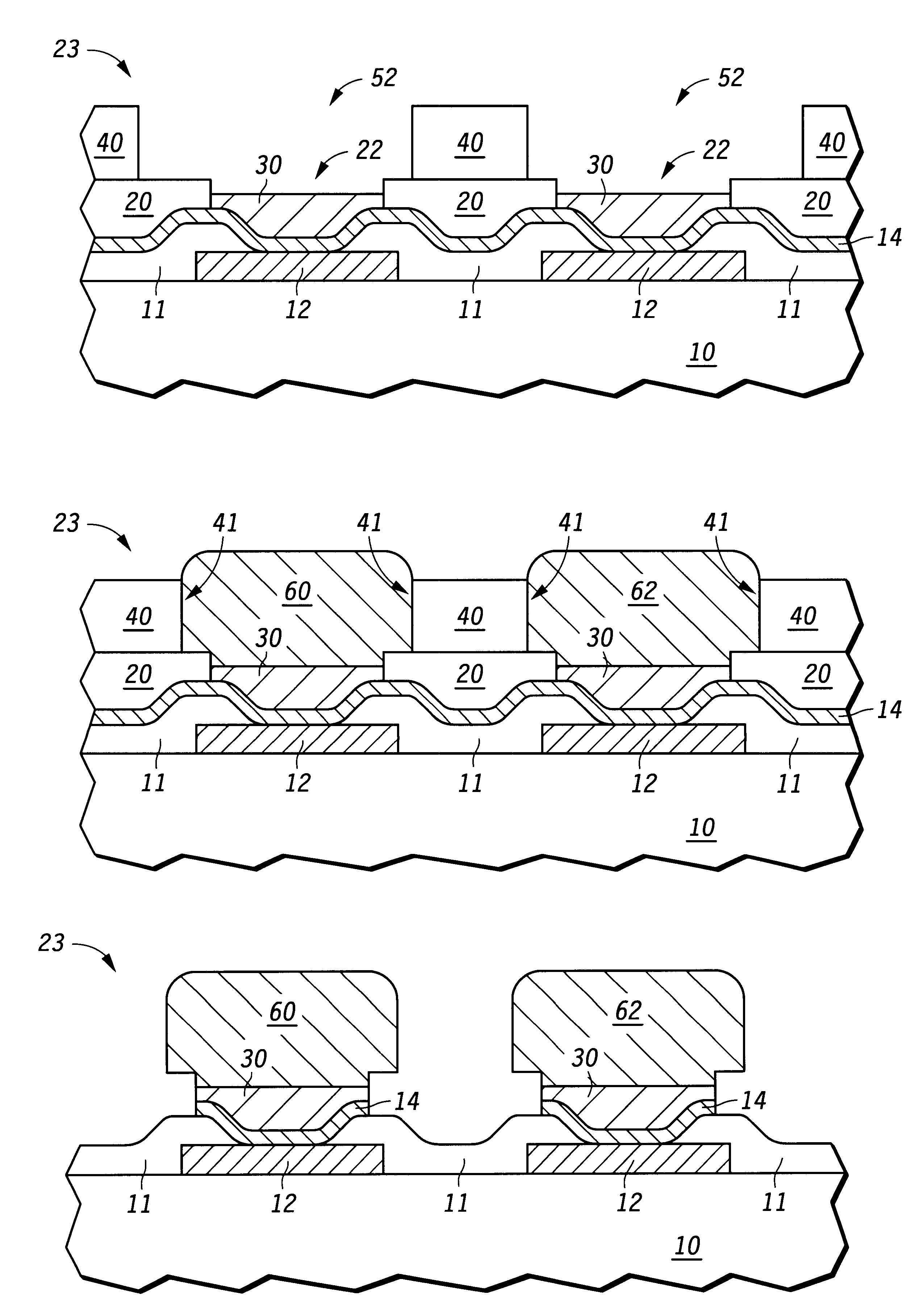
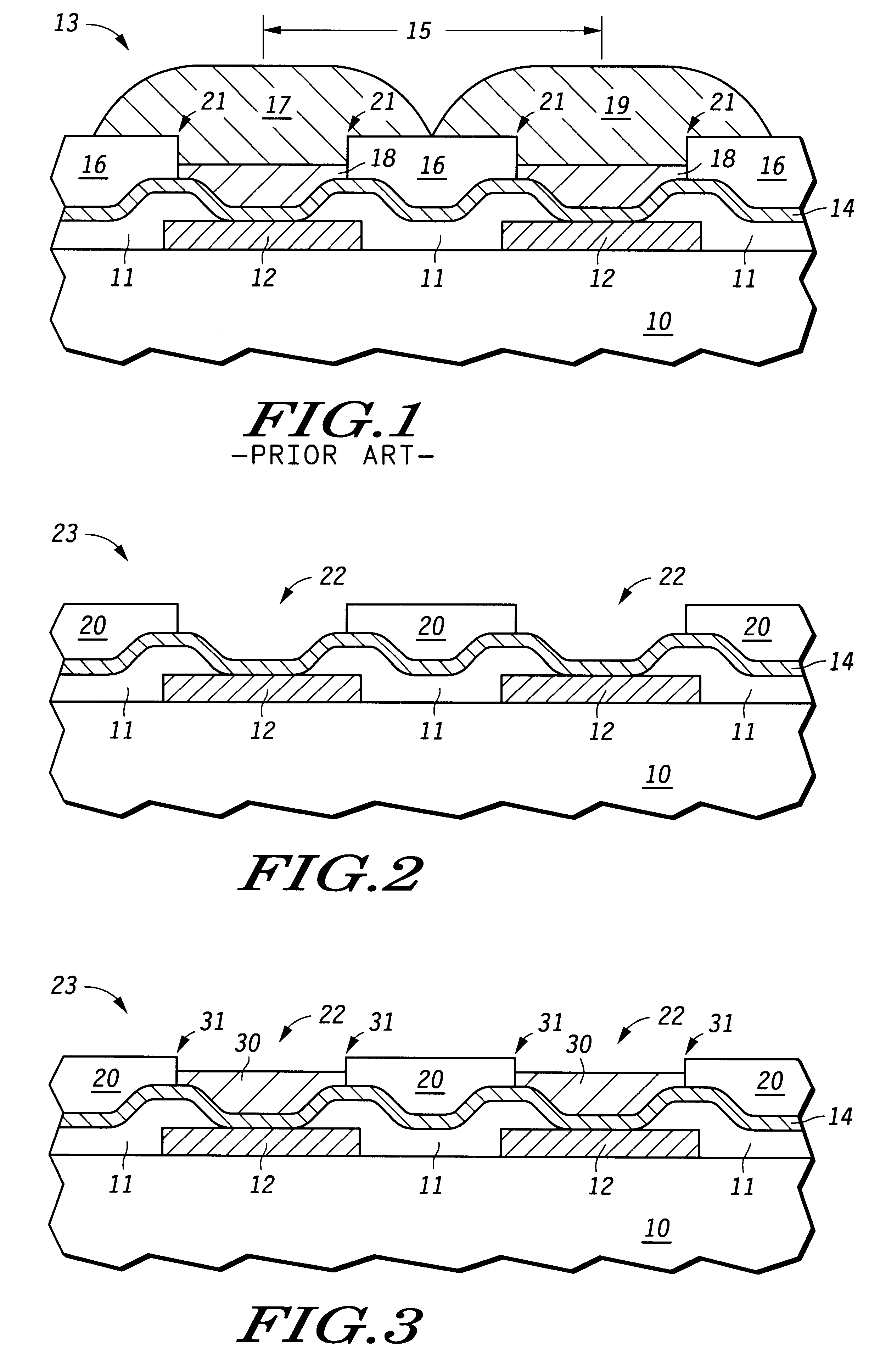
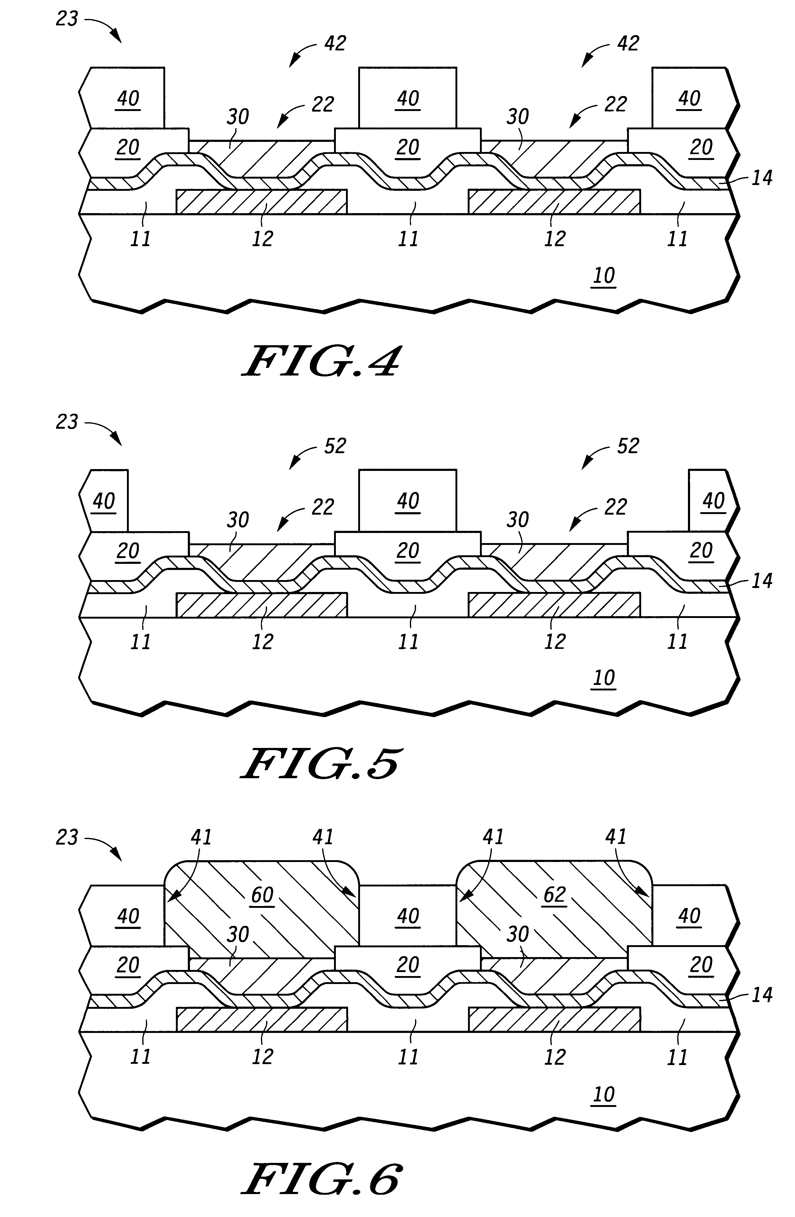
Embodiments of the present invention relate generally to solder bump formation and semiconductor device assemblies. One embodiment, related to a method for forming a bump structure, includes providing a semiconductor device having a bond pad, and forming a first masking layer overlying the bond pad. The first masking layer is patterned to form a first opening overlying at least a portion of the bond pad, and a stud is formed at least within the first opening. A second masking layer is formed overlying the first masking layer and the stud, and the second masking layer is patterned to form a second opening overlying at least a portion of the stud. The method further includes forming a solder bump at least within the second opening.
Another embodiment related to a method for forming a bump structure includes providing a semiconductor device having a bond pad and forming a masking layer overlying the bond pad having a first portion and a second portion. The ...
PUM
| Property | Measurement | Unit |
|---|---|---|
| Thickness | aaaaa | aaaaa |
| Thickness | aaaaa | aaaaa |
| Thickness | aaaaa | aaaaa |
Abstract
Description
Claims
Application Information