Liquid crystal display device comprising an electrode having a connection portion with a dielectric member thereon as to contact a pixel electrode of the second substrate, and manufacturing method for the same
a technology of a dielectric member and a connection portion, which is applied in the direction of non-linear optics, instruments, optics, etc., can solve the problems of abnormal display with a trace of misalignment, and achieve the effects of improving display quality, poor display, and increasing transmittan
- Summary
- Abstract
- Description
- Claims
- Application Information
AI Technical Summary
Benefits of technology
Problems solved by technology
Method used
Image
Examples
first embodiment
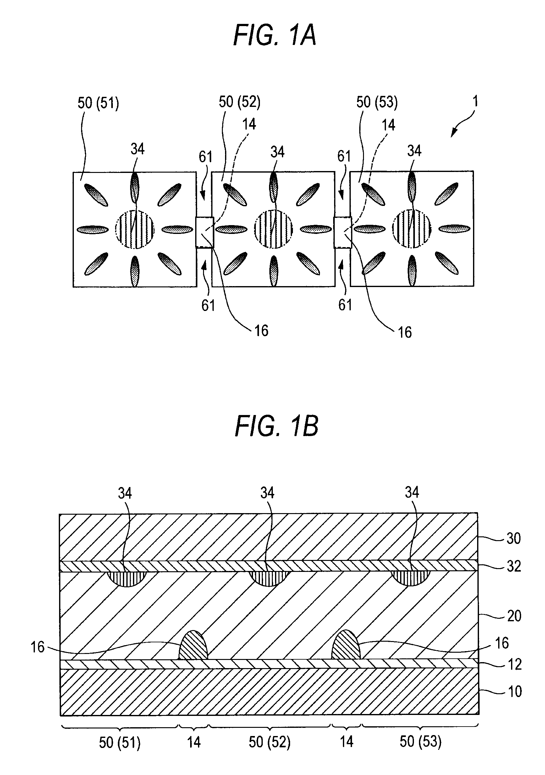
[0032]By referring to a schematic plan layout of FIG. 1A and a main-part cross sectional view of FIG. 1B, described is an embodiment, i.e., first embodiment, of the invention.
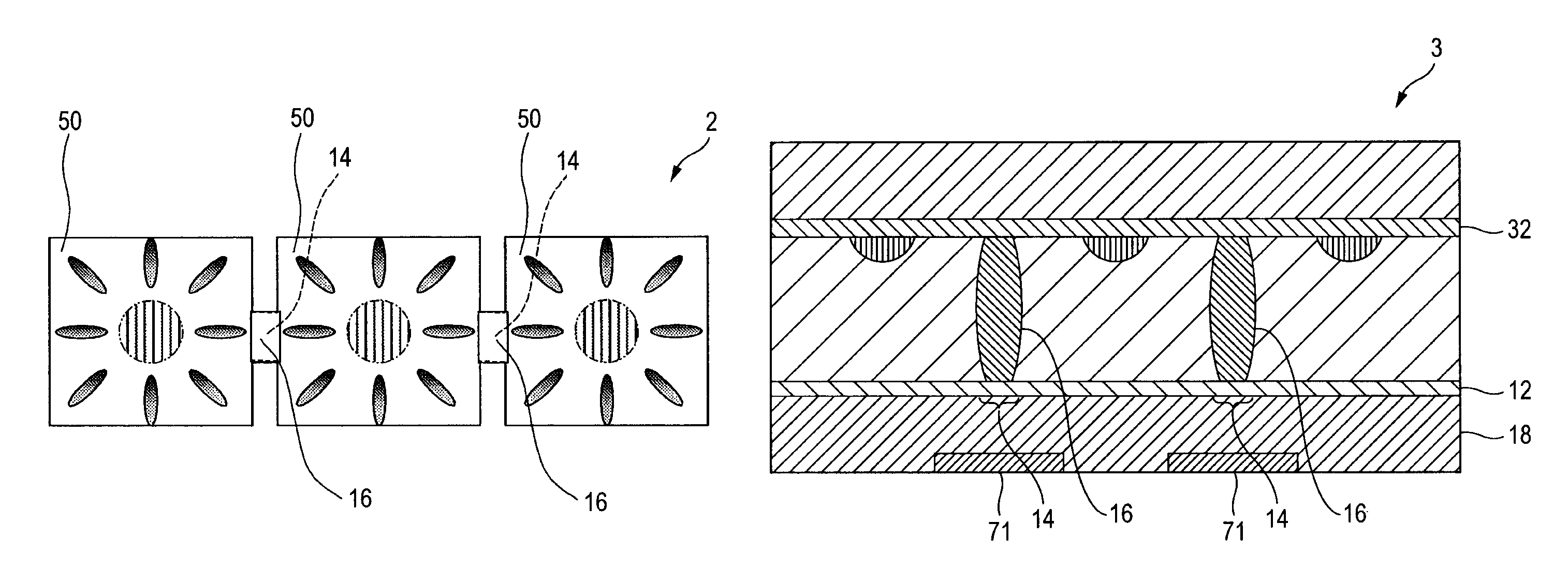
[0033]As shown in FIGS. 1A and 1B, the liquid crystal material of a liquid crystal display device 1 is of a vertical alignment type. In the device, a liquid crystal layer 20 is sealed between opposing substrates 10 and 30, and a plurality of pixels 40 are included for image display. The pixels 40 are each configured by a plurality of sub-pixels 50, e.g., sub-pixels 51, 52, and 53, which are alignment-divided. The sub-pixels 50 are electrically connected to one another by a pixel electrode 12 formed on the substrate 10, and the pixel electrode 12 between the sub-pixels 50 is formed with a notch 61, for example. The pixel electrode 12 between the sub-pixels 50 is formed thereon with a dielectric member 16, and such a portion is hereinafter referred to as connection portion 14.
[0034]The pixel division for alignmen...
second embodiment
[0043]By referring to the schematic plan layout of FIG. 4A showing the positional relationship between a pixel electrode and an alignment control element, and another schematic plan layout of FIG. 4B showing the positional relationship between a pixel electrode and a dielectric member, described next is an embodiment, i.e., a second embodiment, of the invention.
[0044]As shown in FIG. 4A, the connection portion 14 of the pixel electrode 12 is formed to the vertical end portions between any two sub-pixels 50. As shown in FIG. 4B, by forming the dielectric member 16 to the connection portion 14, this configuration also leads to the effect similar to that of the configuration of the dielectric member 16A described by referring to Table 1.
third embodiment
[0045]By referring to the schematic plan layout of FIG. 5A showing the positional relationship between a pixel electrode and an alignment control element, and another schematic plan layout of FIG. 5B showing the positional relationship between a pixel electrode and a dielectric member, described is an embodiment, i.e., a third embodiment, of the invention.
[0046]As shown in FIG. 5A, the connection portion 14 of the pixel electrode 12 is formed entirely to the portion between any two sub-pixels 50. As shown in FIG. 5B, by forming the dielectric member 16 on the connection portion 14, this configuration also leads to the effect similar to that of the configuration of the dielectric member 16A described by referring to Table 1.
[0047]As such, by forming the dielectric member 16 on the pixel electrode 12 (connection portion 14) where the sub-pixels are electrically connected irrespective of the formation position of the connection portion 14, the test result shows that the alignment of th...
PUM
| Property | Measurement | Unit |
|---|---|---|
| width | aaaaa | aaaaa |
| weight | aaaaa | aaaaa |
| electric fields | aaaaa | aaaaa |
Abstract
Description
Claims
Application Information


