Driver apparatus and method
a technology of driving apparatus and driver, which is applied in the direction of electric variable regulation, process and machine control, instruments, etc., can solve the problems of minimal power consumption, impractical large devices for mnb>1/b> and cdac devices, and easy damage, etc., and achieve the effect of maximum curren
- Summary
- Abstract
- Description
- Claims
- Application Information
AI Technical Summary
Benefits of technology
Problems solved by technology
Method used
Image
Examples
first embodiment
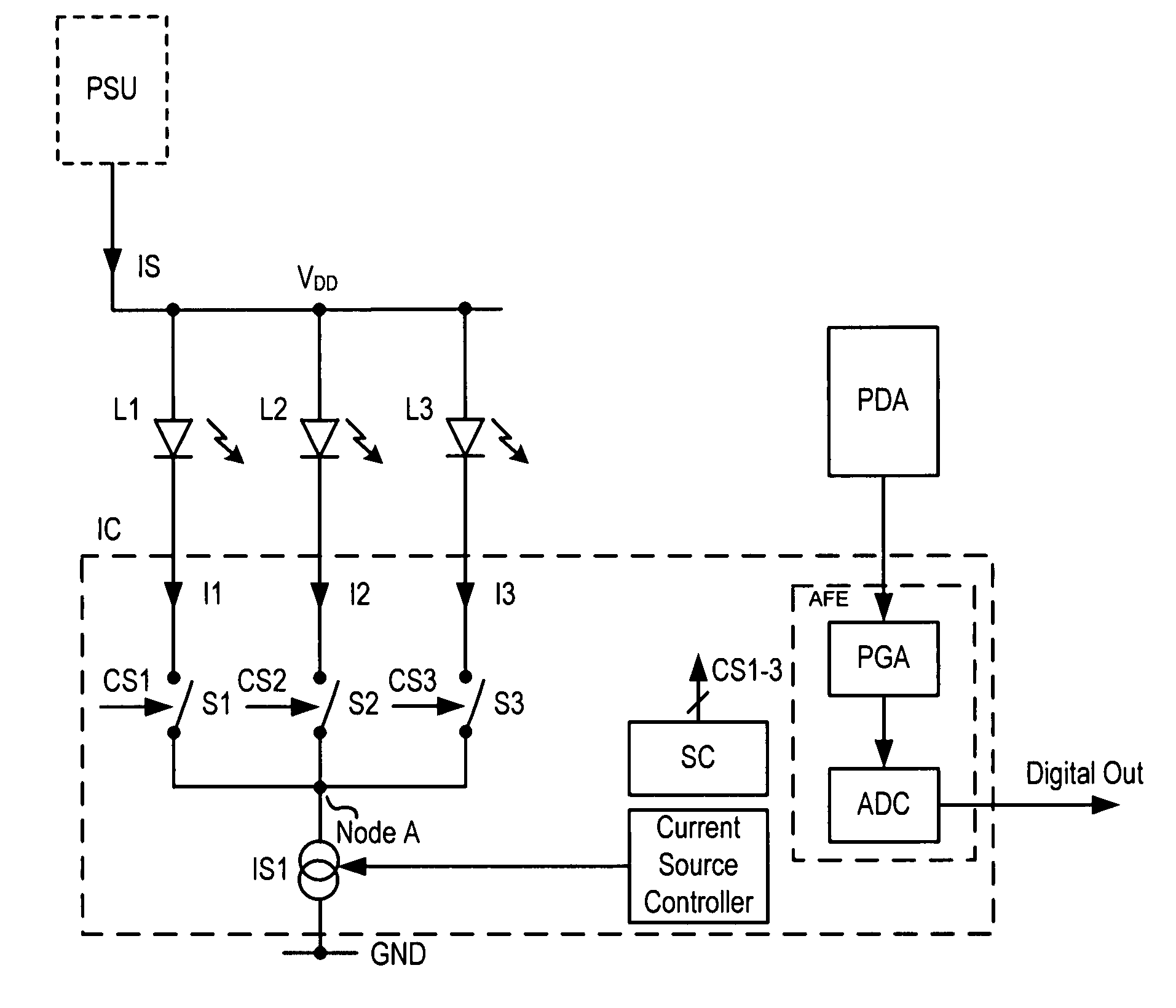
[0052]Thus, it can be seen that in the first embodiment the LED switches (S1-S3) may be integrated on the same IC as the AFE processing circuitry, with the current source IS1 being provided to reduce the generation of unwanted transient signals.
second embodiment
[0053]FIG. 5 shows a basic block diagram of the present invention.
[0054]In a similar manner to FIG. 3, an LED array comprises Red, Green and Blue LEDs L1, L2, L3. The LED switching circuitry S1, S2, S3 is placed on the same monolithic circuit as the analogue front end circuitry (AFE) that drives the switching circuitry. A current source IS1 is provided in the current path between the switches S1, S2, S3 and ground, for controlling the flow of current through the LEDs L1, L2, L3.
[0055]According to the second embodiment a shunt path 50 is provided. The shunt path 50 comprises a switching device S4. The shunt path 50 having the switching device S4 is provided in parallel with the LED array and switching circuitry. The problem relating to the LED switching transients interfering with the ADC is reduced because, as will be explained below, the shunt path 50 enables harmful transitions in the ground current flow to be reduced.
[0056]The following text describes the operation of the switchi...
third embodiment
[0076]FIG. 8 shows a basic diagram of a third embodiment according to the present invention.
[0077]As with FIGS. 3 and 5, an LED array comprises Red, Green and Blue LEDs L1, L2, L3. The LED switching circuitry S1, S2, S3 may form part of the same monolithic circuit as the analogue front end circuitry (AFE) that processes the image data received from the photo sensors. To reduce the problem associated with LED switching transients interfering with the ADC process, a current source IS1 is provided in the current path between the switches S1, S2, S3 and ground, for controlling the flow of current through the LEDs L1, L2, L3. A differential current path 50 (or shunt path) having a switching device S4 is provided in parallel with the array of LEDs and corresponding switches S1-S3.
[0078]In addition, according to this embodiment, a second current source IS2 is provided in the shunt path 50. The second current source IS2 enables the switching of the shunt path 50 to be performed in a more co...
PUM
 Abstract
Description
Claims
Application Information


