
Methods and systems of managing memory addresses in a large capacity multi-level cell (MLC) based flash memory device

a multi-level cell and memory address technology, applied in the field of flash memory devices, can solve the problems of slow flash memory access, limited life of flash memory sectors, and inherent limitations of flash memory

Inactive Publication Date: 2011-02-08
SUPER TALENT TECH CORP
View PDF6 Cites 16 Cited by
  • Summary
  • Abstract
  • Description
  • Claims
  • Application Information

AI Technical Summary

Benefits of technology

This approach enhances data management efficiency, extends device lifespan, and supports high-speed data transfer while ensuring compatibility and environmental resilience, addressing the limitations of MLC flash memory devices.

Problems solved by technology

As such, a problem arises when mobile systems that are designed for one type of flash memory are constructed using another, incompatible type of flash memory.
In addition to the limitations introduced by the USB standard, there are inherent limitations with flash memory.
Also, flash memory sectors have a limited life span; i.e., they can be erased only a limited number of times before failure.
Accordingly, flash memory access is slow due to the erase-before-write nature and ongoing erasing will damage the flash memory sectors over time.

Method used


Image

  • Methods and systems of managing memory addresses in a large capacity multi-level cell (MLC) based flash memory device
  • Methods and systems of managing memory addresses in a large capacity multi-level cell (MLC) based flash memory device
  • Methods and systems of managing memory addresses in a large capacity multi-level cell (MLC) based flash memory device

Examples


Embodiment Construction

[0034]In the following description, numerous details are set forth to provide a more thorough explanation of embodiments of the present invention. It will be apparent, however, to one skilled in the art, that embodiments of the present invention may be practiced without these specific details. In other instances, well-known structures and devices are shown in block diagram form, rather than in detail, in order to avoid obscuring embodiments of the present invention.

[0035]Reference herein to “one embodiment” or “an embodiment” means that a particular feature, structure, or characteristic described in connection with the embodiment can be included in at least one embodiment of the invention. The appearances of the phrase “in one embodiment” in various places in the specification are not necessarily all referring to the same embodiment, nor are separate or alternative embodiments mutually exclusive of other embodiments. Used herein, the terms “upper”, “lower”, “top”, “bottom”, “front”,...


PUM


Abstract

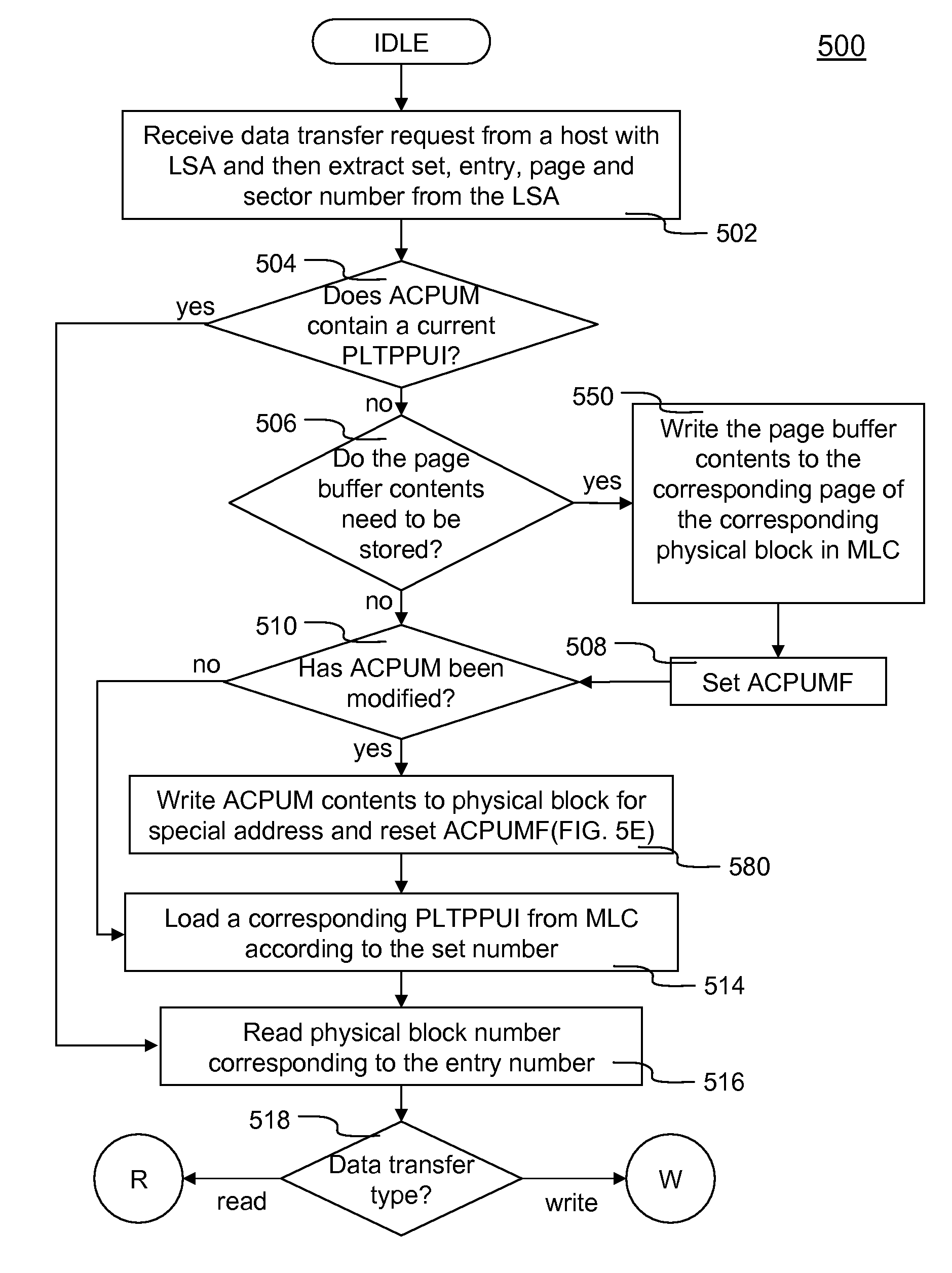
Methods and systems of managing memory addresses in a large capacity multi-level cell based flash memory device are described. According to one aspect, a flash memory device comprises a processing unit to manage logical-to-physical address correlation using an indexing scheme. The flash memory is partitioned into N sets. Each set includes a plurality of entries (i.e., blocks). N sets of partial logical entry number to physical block number and associated page usage information (hereinafter ‘PLTPPUI’) are stored in the reserved area of the MLC based flash memory. Only one the N sets is loaded to address correlation and page usage memory (ACPUM), which is a limited size random access memory (RAM). In one embodiment, static RAM (SRAM) is implemented for fast access time for the address correlation. LSA received together with the data transfer request dictates which one of the N sets of PLTPPUI is loaded into ACPUM.

Description

CROSS-REFERENCE TO RELATED APPLICATIONS[0001]This application is a continuation-in-part (CIP) of co-pending U.S. patent application for “Flash Module with Plane-Interleaved Sequential Writes to Restricted-Write Flash Chips”, Ser. No. 11 / 871,011, filed Oct. 11, 2007, U.S. patent application for “Multi-Channel Flash Module with Plane-Interleaved Sequential ECC Writes and Background Recycling to Restricted-Write Flash Chips”, Ser. No. 11 / 871,627, filed Oct. 12, 2007, and U.S. patent application for “Cell-Downgrading and Reference-Voltage Adjustment for A Multi-Bit-Cell Flash Memory”, Ser. No. 11 / 737,336, filed on Apr. 19, 2007 now U.S. Pat. No. 7,333,364.[0002]This application is also a CIP of U.S. patent application for “Recycling Partially-Stale Flash Blocks Using a Sliding Window for Multi-Level-Cell (MLC) Flash Memory”, Ser. No. 11 / 674,645, filed Feb. 13, 2007 now U.S. Pat. No. 7,620,769, and U.S. patent application for “Two-Level RAM Lookup Table for Block and Page Allocation and ...

Claims


Application Information

Patent Timeline
Patent Type & Authority Patents(United States)
IPC IPC(8): G06F13/16
CPCG06F12/0246G06F12/0607G11C11/5621G11C16/0408G11C16/349G11C16/3495
Inventor LEE, CHARLES C.YU, I-KANGNGUYEN, DAVIDMA, ABRAHAM CHIH-KANGSHEN, MING-SHIANG
Owner SUPER TALENT TECH CORP
Learn More