LED device having improved light output

a technology of led devices and light output, which is applied in the direction of discharge tubes/lamp details, discharge tubes/lamp details, incadescent envelopes/vessels, etc., can solve the problems of increasing manufacturing costs, reducing device efficiency, and high cost of existing patterning methods, for example employing metal shadow masks, etc., and achieves color gamut and reduces the cost of an led device. , the effect of increasing the light outpu

Active Publication Date: 2011-02-22
GLOBAL OLED TECH
View PDF21 Cites 133 Cited by
  • Summary
  • Abstract
  • Description
  • Claims
  • Application Information

AI Technical Summary

Problems solved by technology

Because LED devices employ high-optical-index emissive materials, a large fraction (e.g. greater than 50%) of the emitted light is trapped in the device due to total internal reflection and thus reduces the device efficiency.
However, patterning the materials, particularly for small-molecule organic LED materials is difficult for large-size substrates, thereby increasing manufacturing costs.
Moreover, existing patterning methods, for example employing metal shadow masks, are expensive and can damage deposited organic materials.
However, these disclosures do not address the problem of large amounts of trapped light.
Regardless of the light-emitting layer structure, area LED devices suffer from trapped light in the light-emitting layer, due to the relatively high index of the emission layer compared to air.
While such designs are useful, they require a patterned organic material deposition technology (for example, vacuum deposition through metal shadow-masks) that is difficult to scale to large substrates.
However, the problem of trapped light remains.
The loss of a white emitter reduces the efficiency of the unpatterned device.
Furthermore, the construction of optical cavities tuned to the color of each emitter can be expensive, requiring multiple manufacturing steps.
Such designs, however, do not address the need for reduced manufacturing costs and increased efficiency.
Again, such designs may have increased manufacturing costs due to patterned deposition processes.
Also, significant light may be absorbed by the color filters thereby, reducing efficiency.
However, this design employs a patterned semi-transparent electrode that can be difficult to manufacture in a top-emitting format.
However, there is no teaching of improving device efficiency.
This particular structure requires a patterned reflection film, thereby increasing costs.
The structure is also not useful for unpatterned light-emitting layers.

Method used


Image

  • LED device having improved light output
  • LED device having improved light output
  • LED device having improved light output

Examples


Embodiment Construction

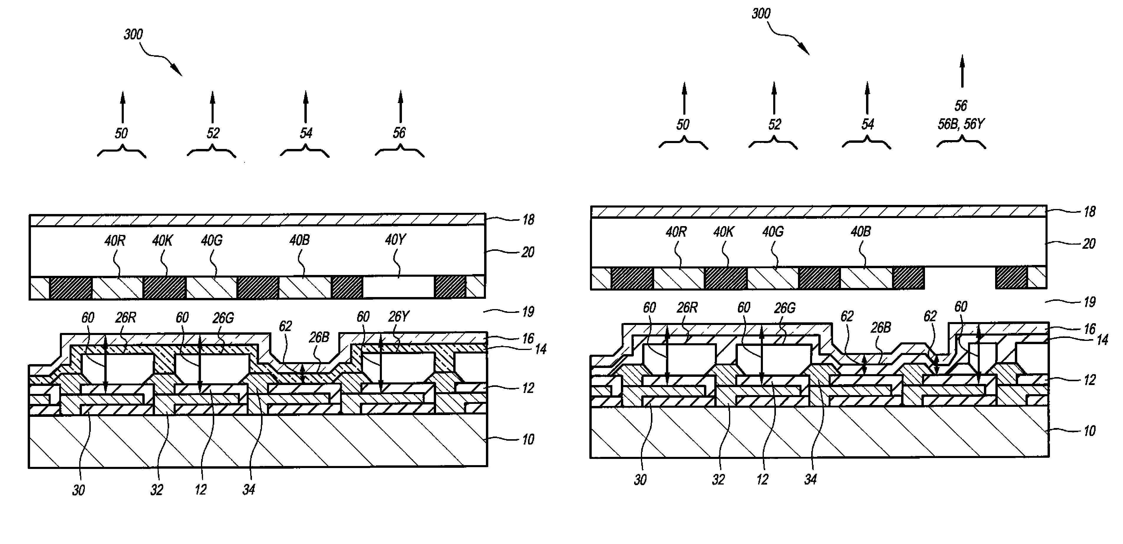
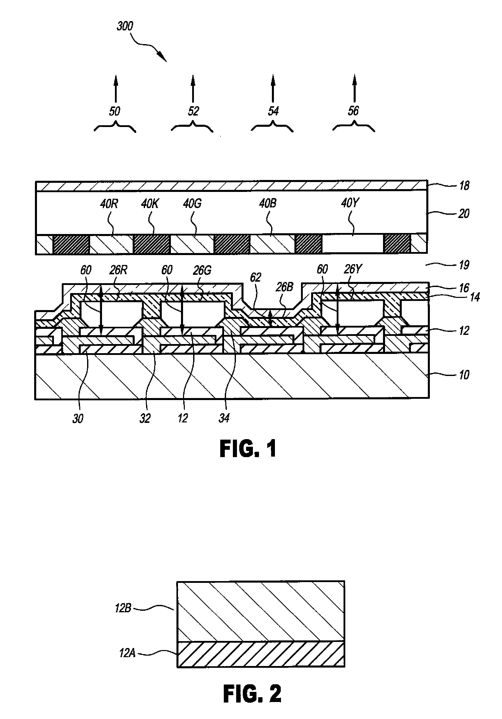
[0022]Referring to FIG. 1, an exemplary embodiment of a light-emitting diode device 300 according to the present invention comprises a first group of sub-pixels (e.g. 50, 52, 56) each comprising a reflective electrode 12 and a second electrode 16 formed over a substrate 10 with an unpatterned light-emitting layer 14 formed between the reflective electrode 12 and the second electrode 16 to comprise a first optical cavity 60 having a first cavity length, and wherein either the reflective 12 or second electrode 16 is patterned to form two or more independently-controllable, light-emitting sub-pixels (e.g. 50, 52, 56). A second group of sub-pixels (e.g. 54) each comprising a reflective electrode 12 and a second electrode 16 formed over the substrate 10 with the unpatterned light-emitting layer 14 formed between the reflective electrode 12 and the second electrode 16 to comprise a second optical cavity 62 having a second cavity length different from the first cavity length of the first o...


PUM


Abstract

A light-emitting diode device that includes a first group of sub-pixels each subpixel comprising a reflective electrode and a second electrode formed over a substrate with an unpatterned light-emitting layer formed between the reflective electrode and the second electrode, thus forming a first optical cavity having a first cavity length. Either the reflective or second electrode is patterned to form two or more independently-controllable, light-emitting sub-pixels. A second group of sub-pixels, each comprising a reflective electrode and a second electrode formed over the substrate. An unpatterned light-emitting layer is formed between the reflective electrode and the second electrode to comprise a second optical cavity having a second cavity length different from the first cavity length of the first optical cavity. Either the reflective or second electrode is patterned to form one or more independently-controllable, light-emitting sub-pixels.

Description

[0001]The present invention relates to light-emitting diode (LED) devices, and more particularly, to LED device structures for improving light output efficiency, improved power distribution, and reduced manufacturing costs.BACKGROUND OF THE INVENTION[0002]Emissive flat-panel display devices are widely used in conjunction with computing devices and in particular with portable devices. These displays are often used in public areas with significant ambient illumination and are viewed from a wide variety of angles.[0003]Light emitting diodes (LED) incorporating thin films of organic or inorganic light-emitting materials have many advantages in a flat-panel display device and are useful in optical systems. U.S. Pat. No. 6,384,529 issued May 7, 2002 to Tang et al. shows an OLED color display that includes an array of organic LED light-emitting elements (pixels). Light is emitted from a pixel when a current is passed through an organic material, the frequency of the light is dependent on t...

Claims


Application Information

Patent Timeline
Patent Type & Authority Patents(United States)
IPC IPC(8): H01J1/62H01J63/04
CPCH01L51/5265H01L27/3213H01L27/322H01L27/3244H01L51/5036H10K59/351H10K59/38H10K59/12H10K50/125H10K50/852
Inventor COK, RONALD S.
Owner GLOBAL OLED TECH
Why Eureka
Try Eureka