Optical semiconductor device and method of controlling the same

a technology of optical semiconductor devices and control data, which is applied in the direction of semiconductor lasers, instruments, optical elements, etc., can solve the problems of 1 oscillating at a wavelength, and achieve the effects of reducing the number of control data, simplifying the generation of control data, and reducing hardware resources during the use of optical semiconductor devices

Active Publication Date: 2011-02-22
SUMITOMO ELECTRIC DEVICE INNOVATIONS
View PDF6 Cites 5 Cited by
  • Summary
  • Abstract
  • Description
  • Claims
  • Application Information

AI Technical Summary

Benefits of technology

[0011]With the method, peaks in reflection peak intensity of an optical waveguide formed with the first segment and the second segment are alternately reduced because of antiphase peaks of reflection peak intensity of the third segment and the first segment and antiphase peaks of reflection peak intensity of the third segment and the second segment. That is, the intensity of the reflection peaks having desirable reflection intensity is alternately reduced. Further, the intensity of the antiphase peaks is increased because there are a plurality of the third segments. This results in increase of the wavelength interval of the reflection peak having the desirable reflection peak intensity. It is therefore possible to restrain the laser oscillation at a wavelength other than the desirable wavelength.
[0013]With the method, the number of the control data may be reduced. In this case, the generation of the control data may be simplified. And hardware resource during the use of the optical semiconductor device may be reduced.

Problems solved by technology

However, the laser disclosed in Document 1 may oscillate at a wavelength other than a desirable wavelength because of regression wavelength caused by the vernier effect.

Method used


Image

  • Optical semiconductor device and method of controlling the same
  • Optical semiconductor device and method of controlling the same
  • Optical semiconductor device and method of controlling the same

Examples


first embodiment

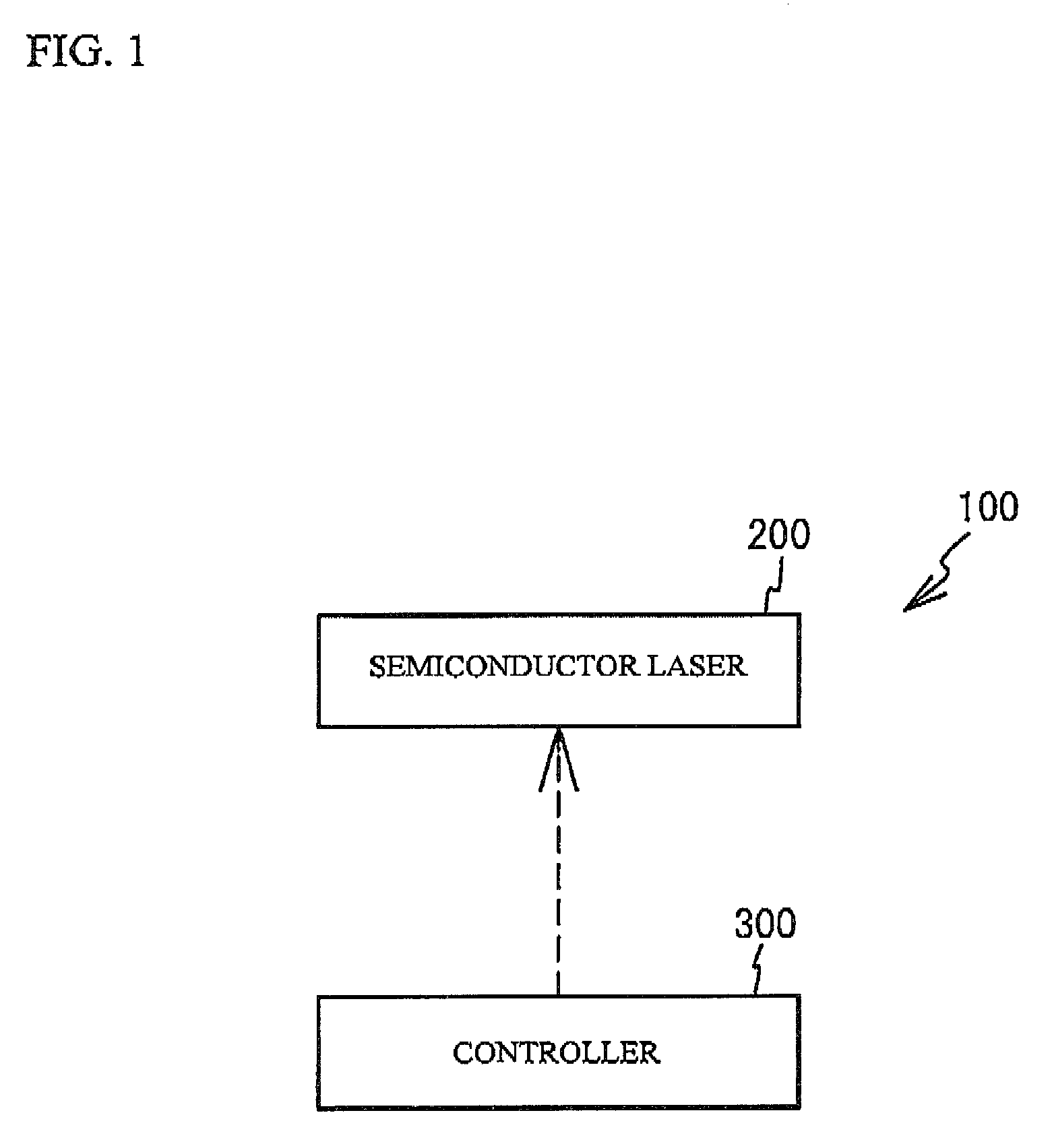
[0023]FIG. 1 illustrates a laser device 100 in accordance with a first embodiment of the present invention. As shown in FIG. 1, the laser device 100 has a semiconductor laser 200 and a controller 300. The controller 300 has a central processing unit (CPU), a random access memory (RAM), a read only memory (ROM) and so on. The ROM of the controller 300 stores control information, a control program and so on of the semiconductor laser 200. The controller 300 controls a laser oscillation wavelength of the semiconductor laser 200 with an electrical signal such as a current provided to the semiconductor laser 200.

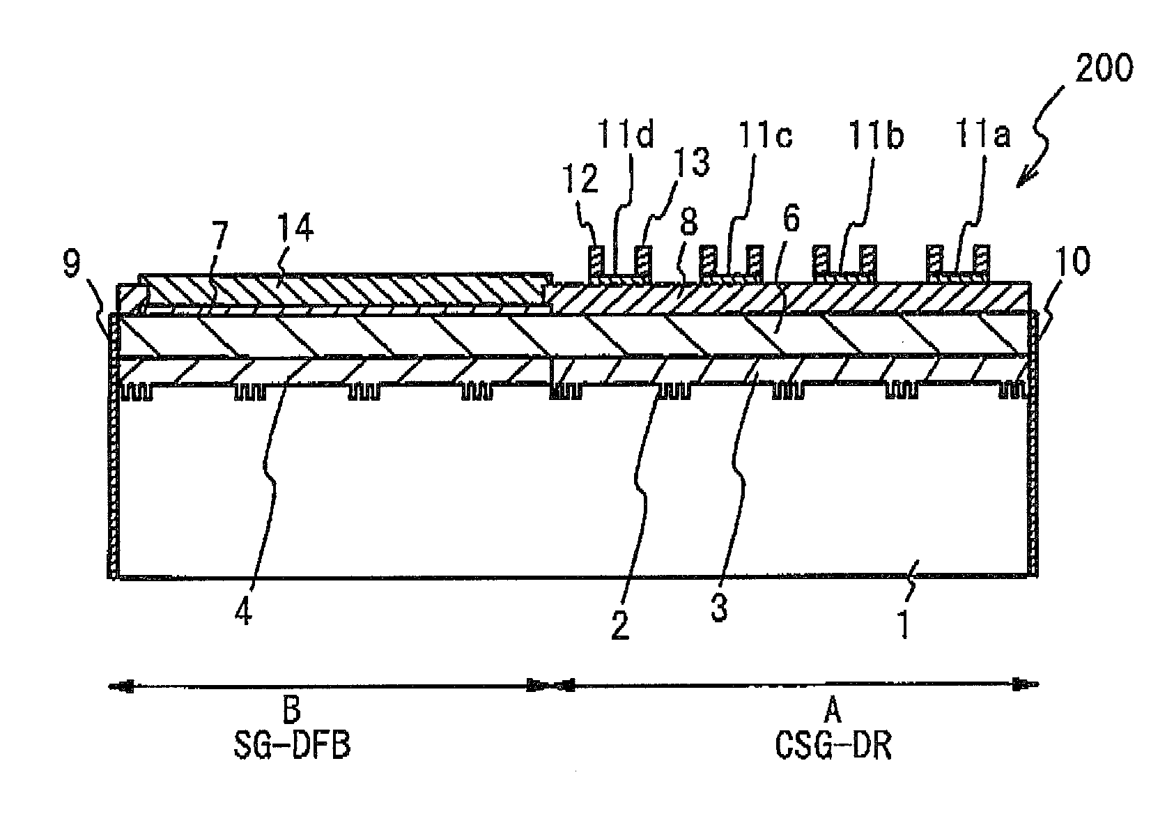
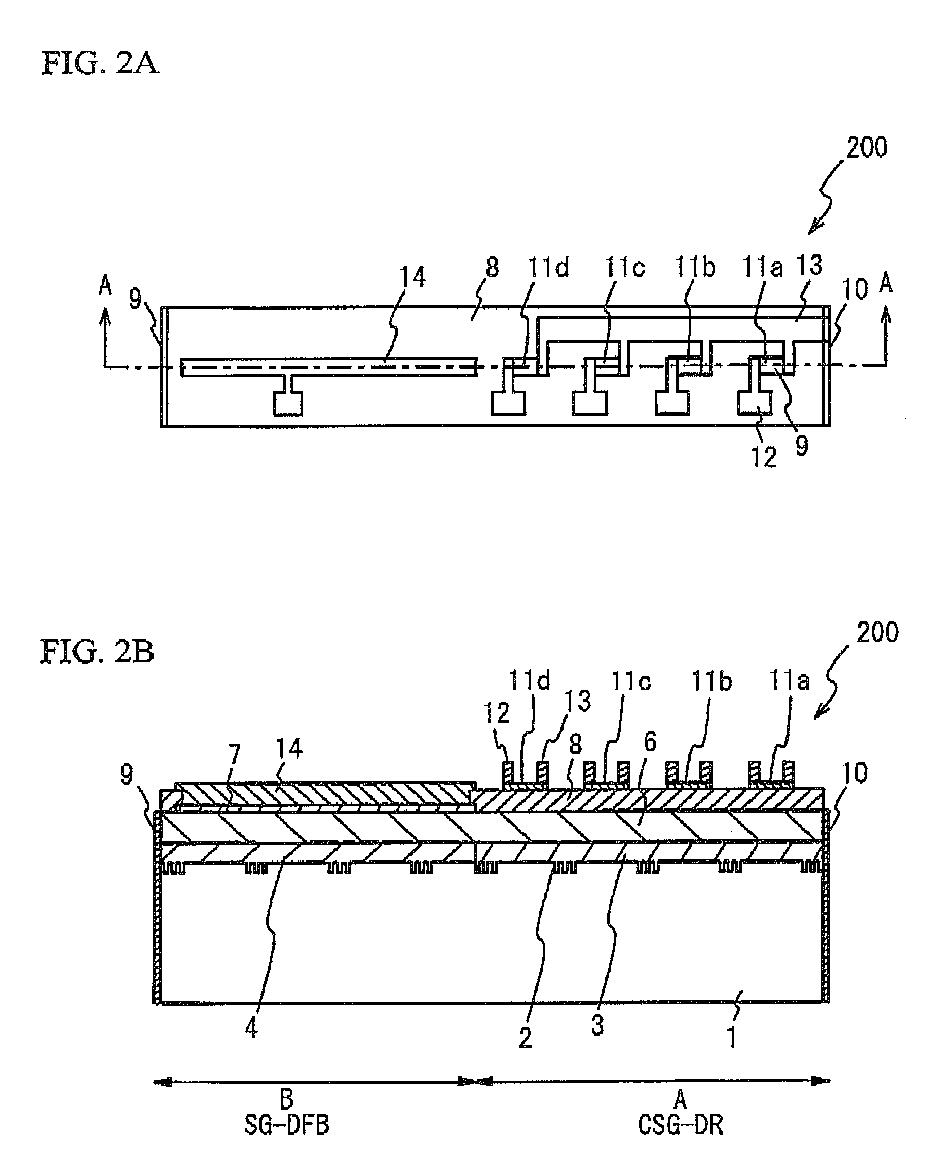
[0024]FIG. 2A and FIG. 2B illustrate details of the semiconductor laser 200. FIG. 2A illustrates a top view of the semiconductor laser 200. FIG. 28 illustrates a cross sectional view taken along a line A-A of FIG. 2A. A description will be given, with reference to FIG. 2A and FIG. 2B, of the semiconductor laser 200. As shown in FIG. 2A and FIG. 2B, the semiconductor laser 200 has...

second embodiment

[0058]Next, a description will be given of a semiconductor laser 200a in accordance with a second embodiment of the present invention. FIG. 5 illustrates a schematic cross sectional view of the semiconductor laser 200a. As shown in FIG. 5, the semiconductor laser 200a has an optical power control (PC) region C, being different from the semiconductor laser 200 shown in FIG. 1.

[0059]The PC region C has a structure in which a waveguide core 5, the cladding layer 6, a contact layer 15 and an electrode 16 are laminated on the substrate 1 in order. In the embodiment, the low reflecting coating 9 is provided on end faces of the substrate 1, the waveguide core 5 and the cladding layer 6 at the PC region C side.

[0060]The substrate 1 and the cladding layer 6 of the CSG-DR region A, the SG-DFB region B and the PC region C are a single layer formed as a unit respectively. The waveguide cores 3, 4 and 5 are formed on a same plane and form a single waveguide core together. The insulating layer 8 ...

third embodiment

[0063]Next, a description will be given of a semiconductor laser 200b in accordance with a third embodiment of the present invention. FIG. 6 illustrates a schematic cross sectional view of the semiconductor laser 200b. As shown in FIG. 6, the semiconductor laser 200a has a Sampled Grating Distributed Reflector (SG-DR) region D instead of the SG-DFB Region B, and further has a Gain region E and a Phase Shift (PS) region F. In the semiconductor laser 200b, the Gain region E and the PS region F are combined to each other between the CSG-DR region A and the SG-DR region D.

[0064]The SG-DR region D has a structure in which a waveguide core 17, the cladding layer 6 and the insulating layer 8 are laminated in order on the substrate 1. The Gain region E has a structure in which a waveguide core 18, the cladding layer 6, a contact layer 19 and an electrode 20 are laminated in order on the substrate 1. The PS region F has a structure in which a waveguide core 21, the cladding layer 6, a contac...


PUM


Abstract

An optical semiconductor device includes a waveguide having one or more first segments having a region that includes a diffractive grating and another region combined to the region, one or more second segments having a region that includes a diffractive grating and another region combined to the region and a plurality of third segments having a region the includes a diffractive grating and another region combined to the region, a length of the second segment being different from that of the first segment, a length of the third segment being shown as L3=L1+(L2−L1)×K1 in which 0.3≦K1≦0.7, L1 is a length of the first segment, L2 is a length of the second segment and L3 is a length of the third segment; and a refractive index control portion controlling refractive index of the first segment through the third segments.

Description

BACKGROUND OF THE INVENTION[0001]1. Field of the Invention[0002]The present invention relates an optical semiconductor device and a method of controlling the same.[0003]2. Description of the Related Art[0004]A wavelength-tunable semiconductor laser lasing some wavelength with a single element is being developed in many organizations, along with a prevalence of Wavelength Division Multiplexing (WDM) communication using an optical fiber. A wavelength-tunable semiconductor laser proposed before now is roughly classified into two types. One of the two types has a Semiconductor Optical Amplifier (SOA) in an external resonator, and controls a lasing wavelength with use of a wavelength selectable portion included in the external resonator. The other of the two types has a structure in which a wavelength-selectable resonator is built in a semiconductor element having a gain with respect to the lasing.[0005]A representative wavelength-tunable semiconductor laser, in which the resonator is bu...

Claims


Application Information

Patent Timeline
Patent Type & Authority Patents(United States)
IPC IPC(8): G02B6/34
CPCH01S5/0612H01S5/06256H01S5/0265H01S5/0287H01S5/0425H01S5/06258H01S5/1039H01S5/1209H01S5/1212H01S5/1215H01S5/125
Inventor FUJII, TAKUYA
Owner SUMITOMO ELECTRIC DEVICE INNOVATIONS
Why Eureka
Try Eureka