Methods for manufacturing a sensor assembly

a sensor and assembly technology, applied in the direction of magnets, magnetic bodies, semiconductor/solid-state device details, etc., can solve the problems of unsuitable methods, inability to use acf/acp on uneven surfaces such as rigid pcb boards assembled, and inability to manufacture acf/acp at low temperature, so as to avoid the risk of creating

Active Publication Date: 2011-03-15
MICROSOFT TECH LICENSING LLC
View PDF15 Cites 0 Cited by
  • Summary
  • Abstract
  • Description
  • Claims
  • Application Information

AI Technical Summary

Benefits of technology

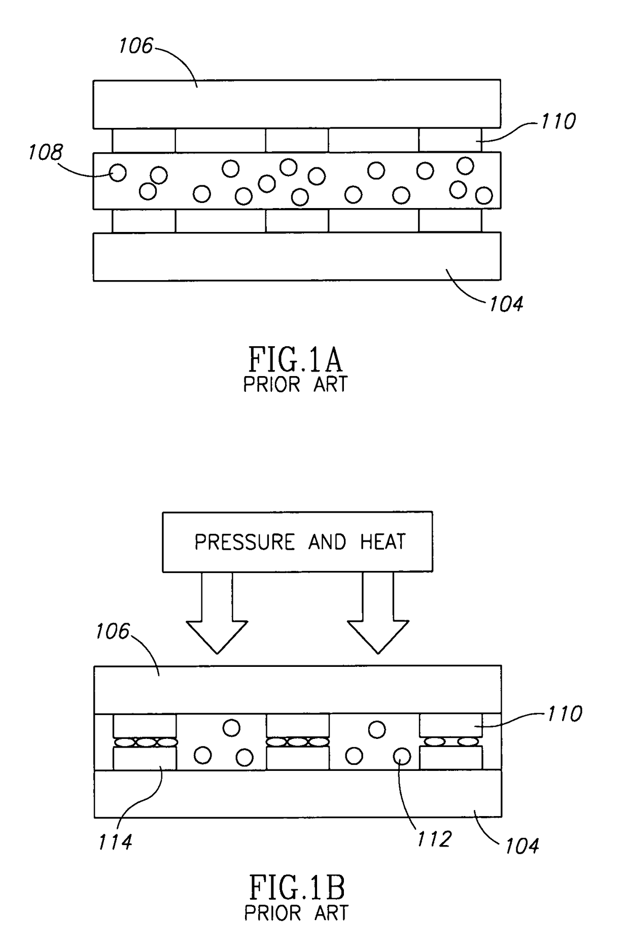
[0014]An aspect of some embodiments of the invention relates to methods for creating electrical and mechanical contacts between electrical components, having located thereon electrical pads, using a conductive material, such as adhesive, while avoiding the risk of creating lateral conductance between the pads. In an exemplary embodiment of the invention, the electrical pads are located on polymeric / heat sensitive substrates, such as PET foils, as well as brittle components, such as PCBs. In some exemplary embodiments of the invention, at least one non-conductive spacer is used to avoid creating lateral conductance between the pads. Optionally, the non-conductive spacer is located on a PCB. Optionally, the non-conductive spacer is located on a sensor. Optionally, a conductive adhesive is applied to the pads subsequent to the placement of the non-conductive spacer. The spacer is operative, in some embodiments of the invention, to act as a blocking element to stop lateral flow of the conductive epoxy.
[0015]In some exemplary embodiments of the invention, a conductive spacer is used as part of the contact mechanism, avoiding any lateral conductance between the pads. Optionally, at least one conductive spacer is placed on a pad. Since for use as a spacer, the conductive spacer is required to be coherent and, when conductive epoxy is used, should be cured before assembly, optionally a supplemental coating of a conductive adhesive is placed on the conductive spacer prior to assembly. Since the spacer is conductive and forms part of the contact, only a small amount of epoxy is used, making it easier to avoid lateral flow to the next spacer.
[0017]An aspect of some exemplary embodiments of the invention relates to methods of manufacturing a sensor assembly. Optionally, the sensor assembly is a component of a digitizer, a personal computer, a personal data assistant or a mobile phone. In an exemplary embodiment of the invention, a sensor array and at least one PCB are connected together electrically and / or mechanically while avoiding creating lateral conductance between electrical pads located thereon. In an exemplary embodiment of the invention, the connected sensor array and at least one PCB are secured within a frame. Optionally, the frame provides mechanical stability to the sensor assembly. Optionally, the frame provides a recess for locating a peripheral coil. In some exemplary embodiments of the invention, the frame is provided with alignment extensions to assist with aligning the frame with another object, such as an LCD screen. In an exemplary embodiment of the invention, a peripheral coil is placed within the recess of the frame. Optionally, the peripheral coil is constructed of a conductive material, such as copper. Optionally, the peripheral coil is wound about the frame in order to position it within the recess. Optionally, one end of the peripheral coil is connected to a first set of electrical pads and a second end of the peripheral coil is connected to a second set of electrical pads. In an exemplary embodiment of the invention, the sensor array, PCB, frame and peripheral coil are encapsulated in a non-conductive material to improve the mechanical stability of the assembly and to help secure the peripheral coil in place.
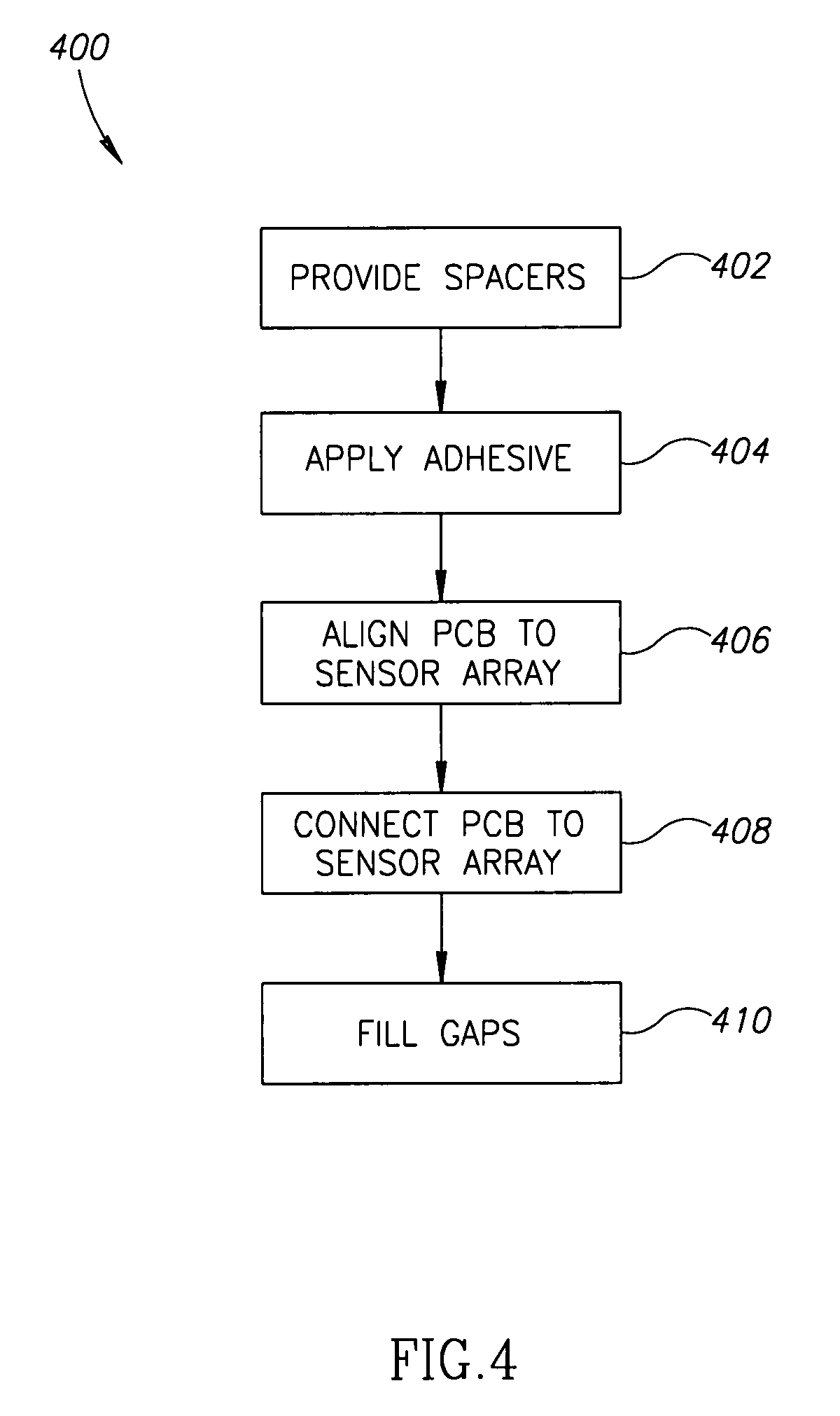
[0018]There is thus provided in accordance with an exemplary embodiment of the invention, a method for connecting substrates having electrical conductive elements thereon, comprising: providing at least one spacer between the substrates; applying a conductive material to at least one of the electrical conductive elements; aligning the electrical conductive elements; and, connecting the substrates by urging them together, wherein the at least one spacer prevents lateral spreading of the conductive material on the substrates from bridging a distance between adjacent conductive elements during the connecting. In some exemplary embodiments of the invention, the method further comprises filling in gaps between the substrates. Optionally, the gaps are filled in with a non-conductive adhesive. Optionally, at least one of the substrates is a PCB. Optionally, at least one of the substrates is a sensor array. Optionally, at least one spacer is non-conductive. Optionally, at least one spacer is conductive. Optionally, at least some of the conductive spacers are comprised in the conductive elements. Optionally, at least one non-conductive spacer is planar. Optionally, at least one non-conductive spacer is elongate. Optionally, the planar spacer prevents lateral spread by blocking the spread. Optionally, at least one spacer determined a distance between the substrates. In some exemplary embodiments of the invention, at least one conductive spacer is comprised of a cured conductive material. Optionally, the electrical conductive elements are pads. Optionally, urging is performed by a weight. Optionally, the urging planarizes at least one of the substrates by conforming the electrical component to the at least one spacer. In some exemplary embodiments of the invention, the conductive material is a conductive adhesive.

Problems solved by technology

This method is unsuitable when the electric pads are part of polymeric substrates, such as a PET foil, due to the relatively high temperatures required to practice this option.
These disadvantages make it impossible to use ACF / ACP on uneven surfaces such as rigid PCB boards assembled with electronic components because standard bonding machinery supports limited surface areas and specific geometries.
In addition the ACF / ACP will not allow assembly at low temperature.
However, the use of a conductive adhesive, such as Epo-Tek E4110, is very likely to result in lateral conductance.
Applying even a small amount of pressure to the first substrate 206 will cause the adhesive 202 to spread sideways, in which case, undesirable lateral conductance is likely to occur.

Method used


Image

  • Methods for manufacturing a sensor assembly
  • Methods for manufacturing a sensor assembly
  • Methods for manufacturing a sensor assembly

Examples


Embodiment Construction

[0040]The present invention is best understood when described in conjunction with position detecting systems, such as a digitizer or touch screen. U.S. Pat. No. 6,690,156 and U.S. patent application Ser. No. 10 / 649,708, entitled “Transparent Digitizer”, the disclosures of which are herein incorporated by reference, describe positioning detecting devices located on top of a flat screen display. Some of the exemplary embodiments in both disclosures describe a sensor assembly built of transparent foils containing a matrix of vertical and horizontal conductors. Optionally, the sensor assembly is for use with at least one of: a tablet personal computer (tablet “PC”), a lap-top PC, a personal data assistant (“PDA”) or any hand held device such as a mobile phone. The exemplary embodiments described herein are suitable for manufacturing such a sensor assembly.

[0041]Referring to FIG. 3, an exemplary sensory array 302 is shown in proximity to a first PCB substrate 304 and a second PCB substra...


PUM

PropertyMeasurementUnit
temperatureaaaaaaaaaa
electrical conductiveaaaaaaaaaa
distanceaaaaaaaaaa

Abstract

A method for connecting substrates having electrical conductive elements thereon, comprising: providing at least one spacer between the substrates; applying a conductive material to at least one of the electrical conductive elements; aligning the electrical conductive elements; and, connecting the substrates by urging them together, wherein the at least one spacer prevents lateral spreading of the conductive material on the substrates from bridging a distance between adjacent conductive elements during the connecting.

Description

RELATED APPLICATIONS[0001]This Application is a National Phase of PCT Patent Application No. PCT / IL2005 / 001271 having International Filing Date of Nov. 29, 2005, which claims the benefit of U.S. Provisional Patent Application No. 60 / 631,254 filed on Nov. 29, 2004. The contents of the above Applications are all incorporated herein by reference.FIELD OF THE INVENTION[0002]The present application is concerned with methods for manufacturing a sensor assembly.BACKGROUND OF THE INVENTION[0003]Existing methods of creating electrical and mechanical contacts between conductive pads include soldering, using anisotropic conductive paste (“ACP”) or film (“ACF”), and conductive adhesives.[0004]Soldering is commonly used in the electronics industry. However, in order to create a good electric contact both pads are heated to relatively high temperatures. This method is unsuitable when the electric pads are part of polymeric substrates, such as a PET foil, due to the relatively high temperatures re...

Claims


Application Information

Patent Timeline
Patent Type & Authority Patents(United States)
IPC IPC(8): H01L21/00
CPCH05K3/321H01L2224/16Y10T29/49126H01L2224/83101H01L2924/01079H01L2924/15311H05K3/3452H05K3/361H05K3/368H05K2201/0367H05K2201/09909H05K2201/10977H05K2201/2036H05K2203/1476H01L2224/13016H01L2224/2919H01L2224/83851H01L2224/81903H01L2224/81801Y10T29/49071Y10T29/49155Y10T29/49147Y10T29/4902H01L2924/00014
Inventor KRIMAN, MOSHEYAAKOBY, MERAV
Owner MICROSOFT TECH LICENSING LLC
Why Eureka
Try Eureka