Optical transmitter circuit

a technology of optical transmitter and optical receiver, which is applied in the direction of electromagnetic transmission, electromagnetic transmission, and semiconductor lasers. it can solve the problems of deteriorating extinction ratio, increasing power consumption, and inability to operate at high speed, and achieve desirable extinction ratio, low power consumption, and high speed

Inactive Publication Date: 2011-03-15
PANASONIC CORP
View PDF15 Cites 1 Cited by
  • Summary
  • Abstract
  • Description
  • Claims
  • Application Information

AI Technical Summary

Benefits of technology

[0012]Therefore, an object of the present invention is to provide an optical transmitter circuit which is capable of driving a light emitting element at a high speed with a desirable extinction ratio and a low power consumption, and without waveform deterioration of the optical output.
[0024]According to the present invention, a rising-edge peaking current and a falling-edge peaking current are supplied separately to thereby prevent a deterioration of the optical signal waveform outputted from the light emitting element, whereby the light emitting element can be driven with an intended rising speed and an intended falling speed. Moreover, it is not necessary to increase the DC current for preventing the clipping of the falling-edge peaking current, whereby it is possible to reduce the power consumption and improve the extinction ratio.
[0025]Moreover, in the present invention, the ratio of the clipping current with respect to the instantaneous driving current is set to be less than or equal to a predetermined value, whereby it is possible to realize a high-speed response of a light emitting element and to reduce the power consumption.

Problems solved by technology

Therefore, the light emitting element 101 cannot be operated at a high speed.
However, the solution has problems such as an increase in the power consumption, and deterioration in the extinction ratio, which is the ratio between the high level and the low level of the digital signal.
However, with the conventional light emitting element driving circuit shown in FIG. 22, it is necessary to increase the driving current D of the light emitting element 101 by the amount of current to be pulled by the discharge circuit 104, thereby increasing the power consumption of the circuit.
It is necessary to increase the driving current D so as to prevent clipping, and it is necessary to provide a very large current, which makes the circuit scale impractically large.

Method used


Image

  • Optical transmitter circuit
  • Optical transmitter circuit
  • Optical transmitter circuit

Examples


first embodiment

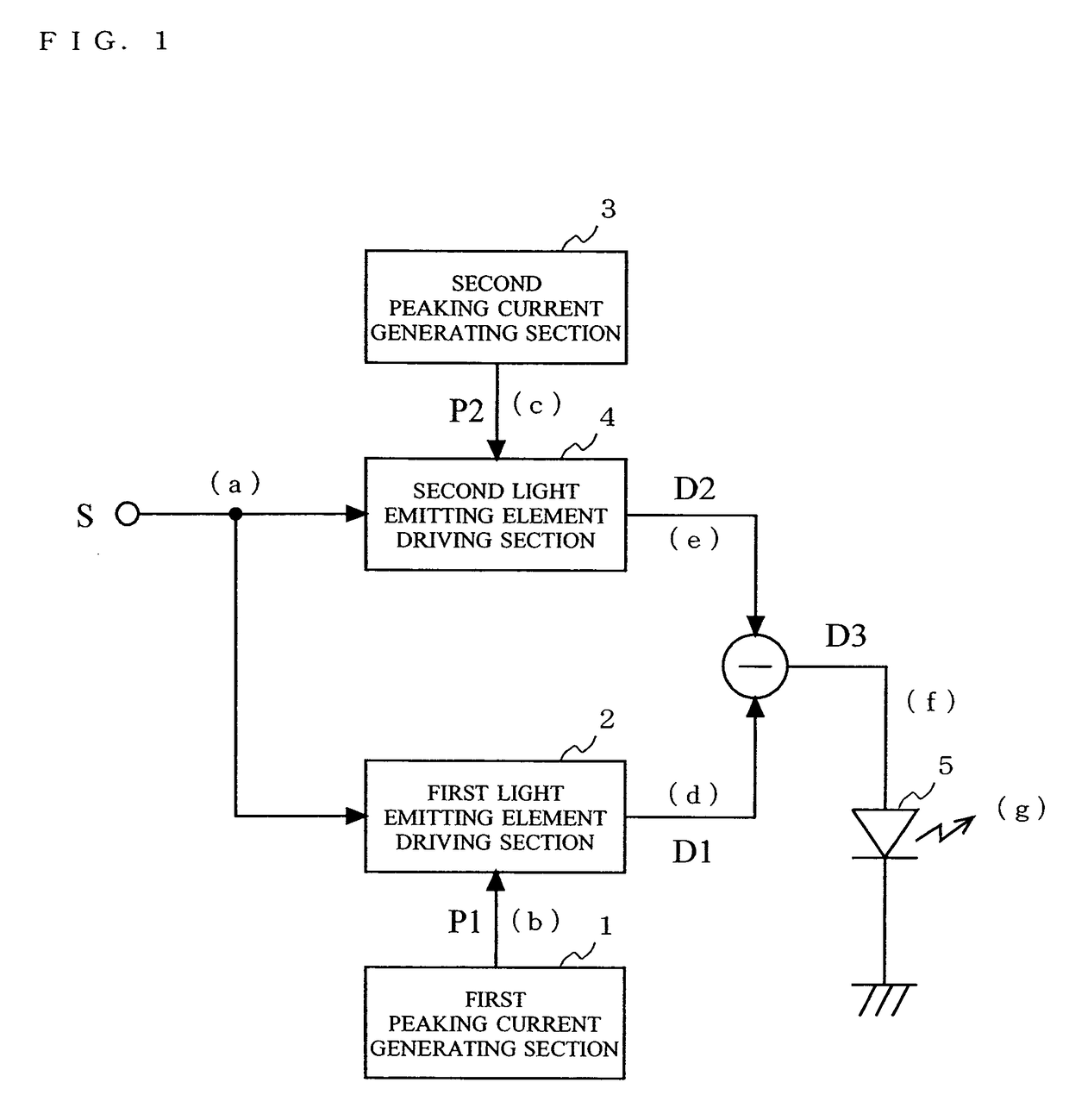
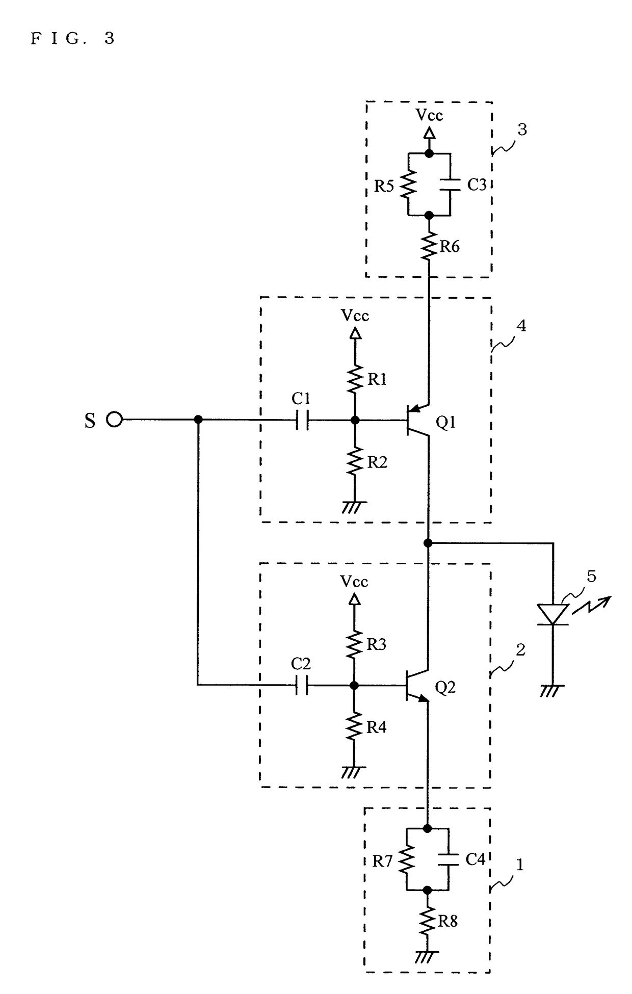
[0057]FIG. 3 shows, in detail, a configuration of an optical transmitter circuit according to the first embodiment of the present invention. In the optical transmitter circuit of the first embodiment, the functional blocks shown in FIG. 1 are each configured as follows.

[0058]The first light emitting element driving section 2 includes a transistor Q2, resistors R3 and R4, and a capacitor C2. The transistor Q2 may be an NPN-type bipolar transistor, an N-channel field effect transistor, or the like. The base of the transistor Q2 is connected to a power supply VCC via the resistor R3 and grounded via the resistor R4, and receives the digital signal S via the capacitor C2. The collector of the transistor Q2 is connected to the light emitting element 5. The resistor R3, the resistor R4 and the capacitor C2 are used for adjusting the DC current through the first light emitting element driving section 2.

[0059]The second light emitting element driving section 4 includes a transistor Q1, resi...

second embodiment

[0065]FIG. 4 shows, in detail, a configuration of an optical transmitter circuit according to the second embodiment of the present invention. The optical transmitter circuit of the second embodiment differs from the optical transmitter circuit of the first embodiment in the configuration of the second light emitting element driving section 4.

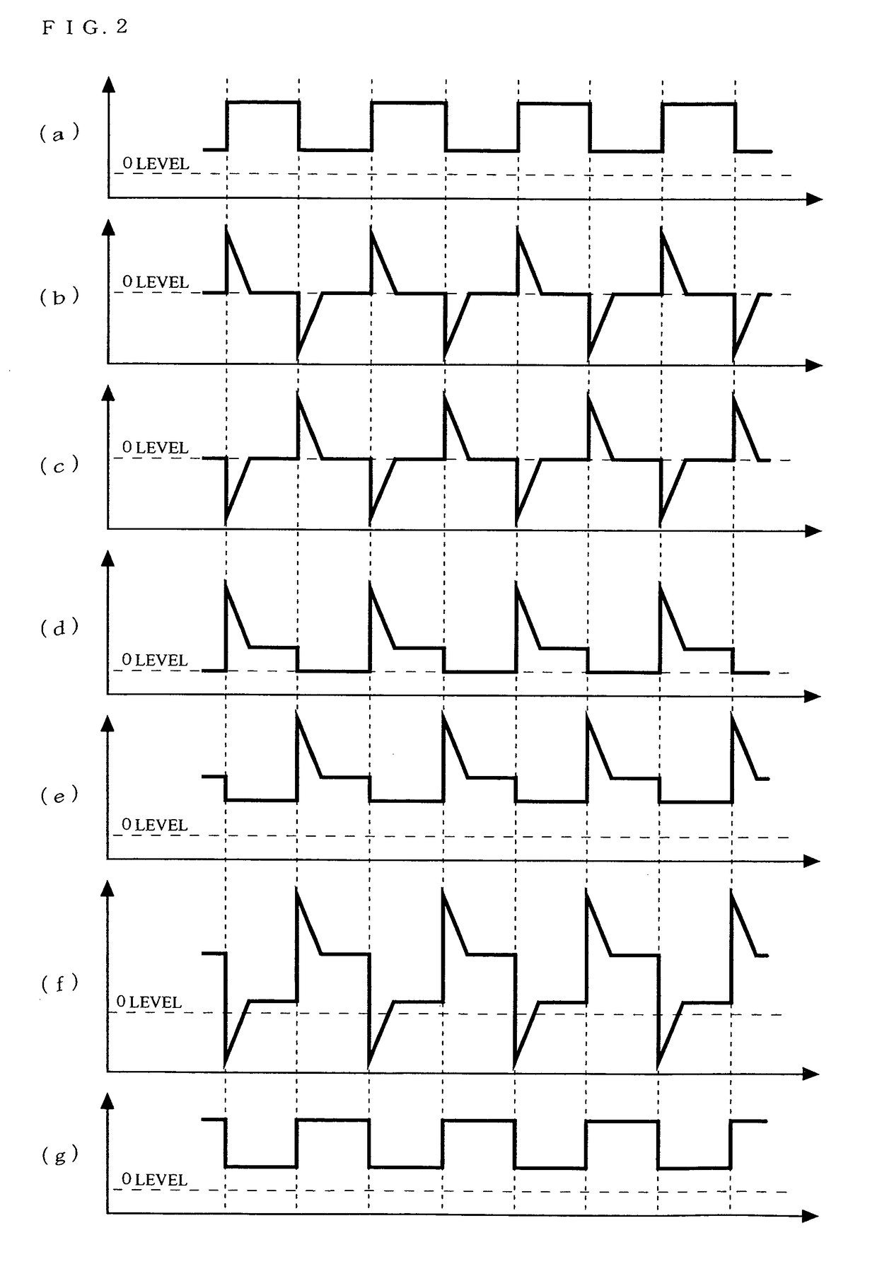
[0066]The second light emitting element driving section 4 includes the transistor Q1, the resistors R1 and R2, and capacitors C1 and C5. The resistor R1, the resistor R2 and the capacitor C1 are used for adjusting the DC current through the second light emitting element driving section 4. The capacitor C5 is inserted between the collector of the transistor Q1 and the light emitting element 5. With such a configuration, the driving current D2 outputted from the second light emitting element driving section 4 when the digital signal S is inputted is an AC component current obtained by cutting the DC component off the current shown in the waveform ...

third embodiment

[0068]FIG. 5 shows, in detail, a configuration of an optical transmitter circuit according to the third embodiment of the present invention. The optical transmitter circuit of the third embodiment differs from the optical transmitter circuit of the first embodiment in the configuration of the first light emitting element driving section 2.

[0069]The first light emitting element driving section 2 includes the transistor Q2, the resistors R3, R4 and R9, and capacitors C2 and C6. The collector of the transistor Q2 is connected to the power supply VCC via a resistor R9, and is connected to the light emitting element 5 via the capacitor C6. With such a configuration, the driving current D1 outputted from the first light emitting element driving section 2 when the digital signal S is inputted is an AC component current obtained by cutting the DC component off the current shown in the waveform (d) of FIG. 2, i.e., only the rising-edge peaking current. The driving current D1 made only of an ...


PUM


Abstract

A first peaking current generating section generates a first peaking current in synchronism with the transitions of a digital signal, being positive at the rising edge and negative at the falling edge. A second peaking current generating section generates a second peaking current in synchronism with the transitions of the digital signal, being negative at the rising edge and positive at the falling edge. A first light emitting element driving section produces a first driving current obtained by combining together a signal amplitude current according to the amplitude of the digital signal and a first peaking current. A second light emitting element driving section produces a second driving current obtained by combining together the signal amplitude current according to the amplitude of the digital signal and a second peaking current. Then, the first and second light emitting element driving sections and drive the light emitting element by using a driving current obtained by subtracting the first driving current from the second driving current.

Description

BACKGROUND OF THE INVENTION[0001]1. Field of the Invention[0002]The present invention relates to an optical transmitter circuit, for use in the field of optical communications, including a circuit capable of driving a light emitting element at a high speed.[0003]2. Description of the Background Art[0004]A commonly known type of a driving circuit for driving, at a high speed, a light emitting element (e.g., an LED) whose response speed is relatively slow employs a peaking technique. With the peaking technique, an instantaneous current (hereinafter referred to as a “peaking current”) is given to a light emitting element so as to force the light emitting element to respond at a high speed. FIG. 20 shows an exemplary configuration of a common conventional light emitting element driving circuit using a peaking technique. FIG. 21 shows waveform diagrams illustrating an operation of the conventional light emitting element driving circuit shown in FIG. 20.[0005]The conventional light emitti...

Claims


Application Information

Patent Timeline
Patent Type & Authority Patents(United States)
IPC IPC(8): H04B10/20
CPCH01S5/06832H04B10/504H04B10/508H01S5/0427
Inventor HASE, KAZUTOSHISASAI, HIROYUKIIEDA, TOMOAKI
Owner PANASONIC CORP
Why Eureka
Try Eureka