Non-volatile memory device and method of fabricating the same

a memory device and non-volatile technology, applied in the field of semiconductor devices, can solve the problems of difficult selection of memory cells from each layer, difficulty in connecting memory cells in different layers, and high manufacturing cost, and achieve the effect of increasing integration

Active Publication Date: 2011-03-22
SAMSUNG ELECTRONICS CO LTD
View PDF4 Cites 50 Cited by
  • Summary
  • Abstract
  • Description
  • Claims
  • Application Information

AI Technical Summary

Benefits of technology

[0007]Example embodiments provide a non-volatile memory device applicable for a multilayer structure to have increased integration. Example embodiments also provide an economical method of fabricating the non-volatile memory device.

Problems solved by technology

However, in a non-volatile memory device having a multilayer structure, connecting memory cells in different layers and selecting memory cells from each layer may be difficult.
In addition, in the non-volatile memory device with a multilayer structure, as the number of stacked layers increases, the manufacturing cost may be higher because more manufacturing processes may be required.

Method used


Image

  • Non-volatile memory device and method of fabricating the same
  • Non-volatile memory device and method of fabricating the same
  • Non-volatile memory device and method of fabricating the same

Examples


Embodiment Construction

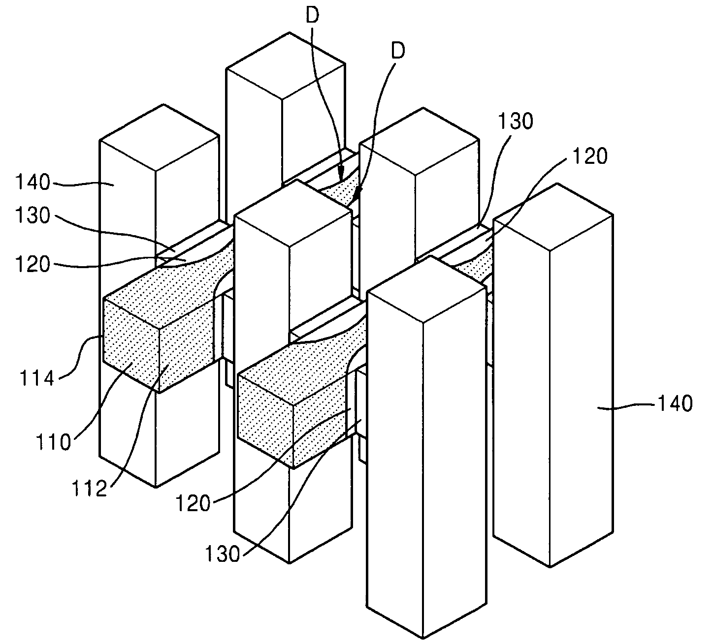
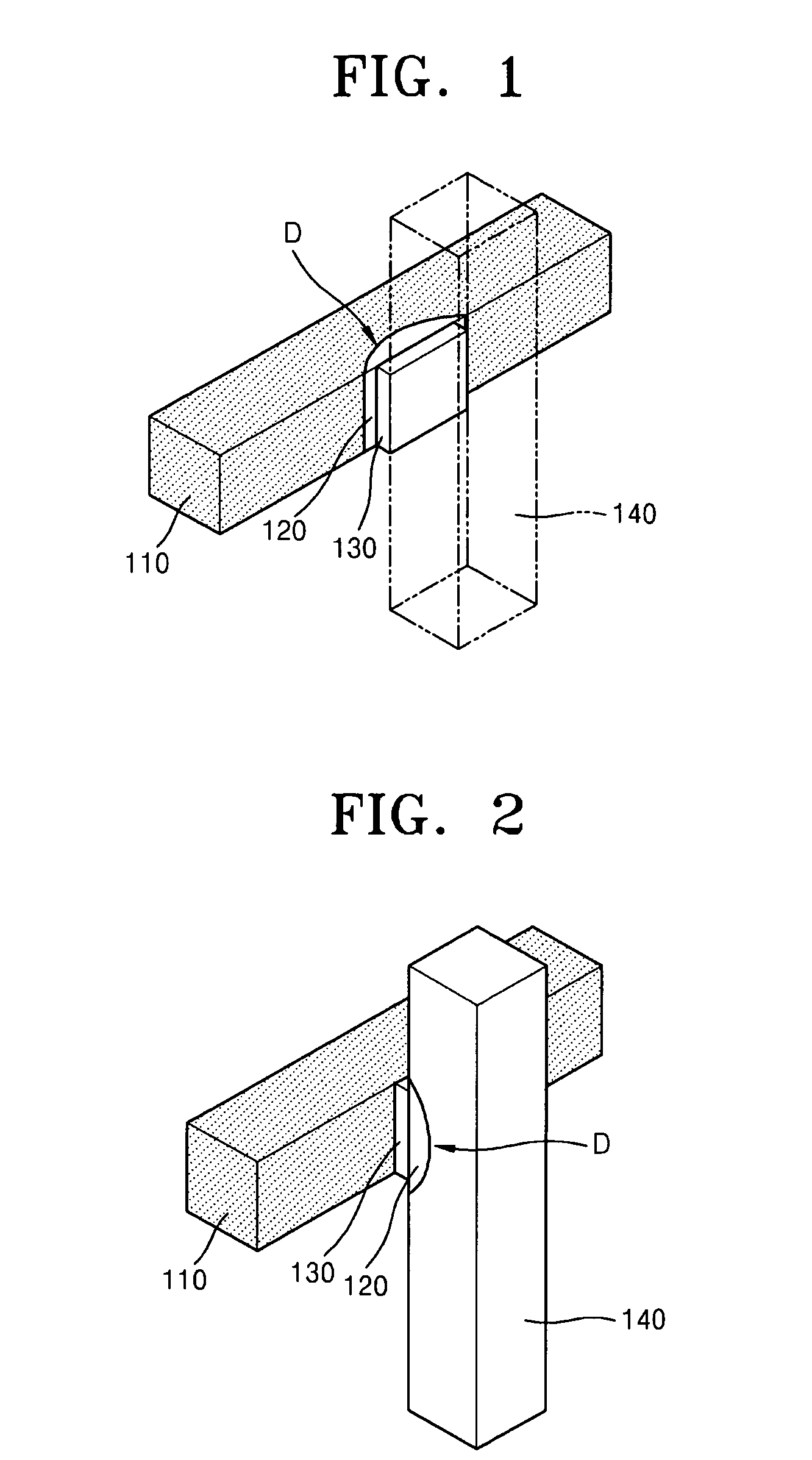
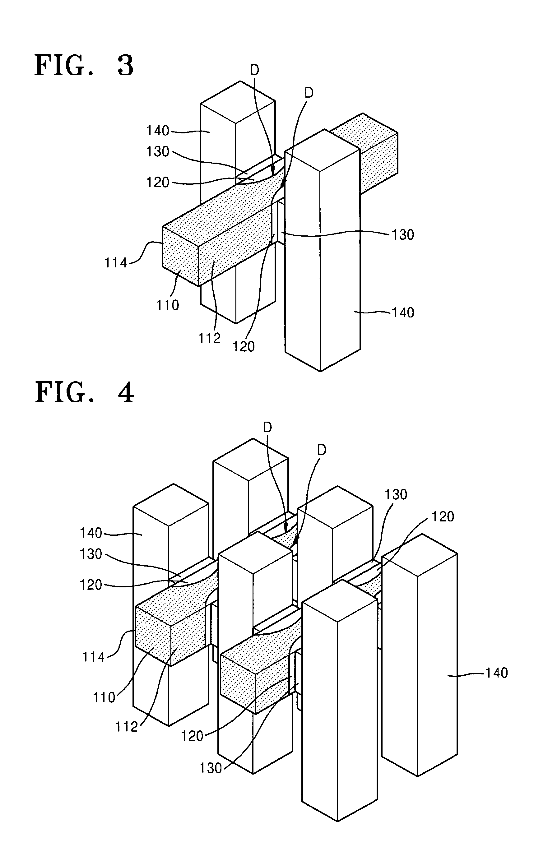
[0025]Hereinafter, example embodiments will be described in detail by explaining example embodiments with reference to the attached drawings. Example embodiments may, however, be embodied in many different forms and should not be construed as being limited to the embodiments set forth herein; rather, these embodiments are provided so that this disclosure will be thorough and complete, and will fully convey the concept of example embodiments to those of ordinary skill in the art. In the drawings, the sizes of elements are exaggerated for clarity.

[0026]It will be understood that when an element is referred to as being “connected” or “coupled” to another element, it can be directly connected or coupled to the other element or intervening elements may be present. In contrast, when an element is referred to as being “directly connected” or “directly coupled” to another element, there are no intervening elements present. As used herein the term “and / or” includes any and all combinations o...


PUM


Abstract

Provided are a non-volatile memory device that may be configured in a stacked structure and may be more easily highly integrated, and a method of fabricating the non-volatile memory device. At least one first electrode and at least one second electrode are provided. The at least one second electrode may cross the at least one first electrode. At least one data storage layer may be at an intersection between the at least one first electrode and the at least one second electrode. Any one of the at least one first electrode and the at least one second electrode may include at least one junction diode connected to the at least one data storage layer.

Description

PRIORITY STATEMENT[0001]This application claims priority under U.S.C. §119 to Korean Patent Application No. 10-2008-0035217, filed on Apr. 16, 2008, in the Korean Intellectual Property Office (KIPO), the entire contents of which are incorporated herein by reference.BACKGROUND[0002]1. Field[0003]Example embodiments relate to a semiconductor device, and more particularly, to a non-volatile memory device having a multilayer structure and a method of fabricating the non-volatile memory device.[0004]2. Description of the Related Art[0005]Demands for semiconductor products with smaller volume and higher data processing capacity have increased. To satisfy these demands, the operation speed and the integration degree of non-volatile memory devices used in semiconductor products has to be increased. In this respect, non-volatile memory devices with a multilayer structure, rather than a conventional monolayer structure, are advantageous for higher integration.[0006]When a multilayer structure...

Claims


Application Information

Patent Timeline
Patent Type & Authority Patents(United States)
IPC IPC(8): H01L45/00
CPCH01L27/249H01L27/2409H01L45/04H01L45/06H01L45/1226H01L45/146H01L45/144H10B63/20H10B63/845H10N70/20H10N70/823H10N70/231H10N70/8828H10N70/8833H10B63/80
Inventor KIM, SUK-PILPARK, YOON-DONGKOO, JUNE-MO
Owner SAMSUNG ELECTRONICS CO LTD
Why Eureka
Try Eureka