High voltage ESD LDMOS-SCR with gate reference voltage

a high-voltage esd and gate reference technology, applied in the direction of semiconductor devices, electrical apparatus, transistors, etc., can solve the problems of high voltage, high voltage protection of esd, encountering problems,

Active Publication Date: 2011-03-22
NAT SEMICON CORP
View PDF3 Cites 25 Cited by
  • Summary
  • Abstract
  • Description
  • Claims
  • Application Information

AI Technical Summary

Problems solved by technology

Electrostatic discharge (ESD) protection of high speed devices such as the protection of switch pins that extend to switch nodes with a fast rise time requirement, encounters problems when it comes to dealing with high voltages.
However, multiple fingers invariably increase the footprint of the device, which implies a large parasitic capacitance associated with the array.
This in turn is incompatible with the fast rise time requirement of the switch node.
Furthermore, in the case of LDMOS-SCR devices it has been found that drain-source avalanche breakdown cannot be used to reliably turn on the device since the extended drain in such a device acts as a saturation resistor which disperses the turn-on voltage.
Therefore snapback of the device cannot be achieved reliably.
Thus, a circuit such as that shown in FIG. 1, which makes use of an LDMOS-SCR 100 to protect a switch node 102, and which relies on avalanche breakdown to turn on, does not provide for a reliable solution.

Method used


Image

  • High voltage ESD LDMOS-SCR with gate reference voltage
  • High voltage ESD LDMOS-SCR with gate reference voltage
  • High voltage ESD LDMOS-SCR with gate reference voltage

Examples


second embodiment

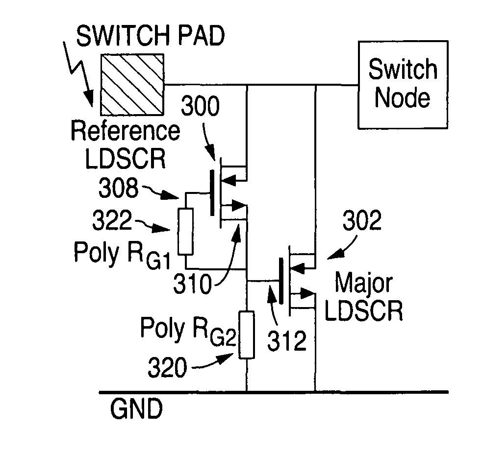
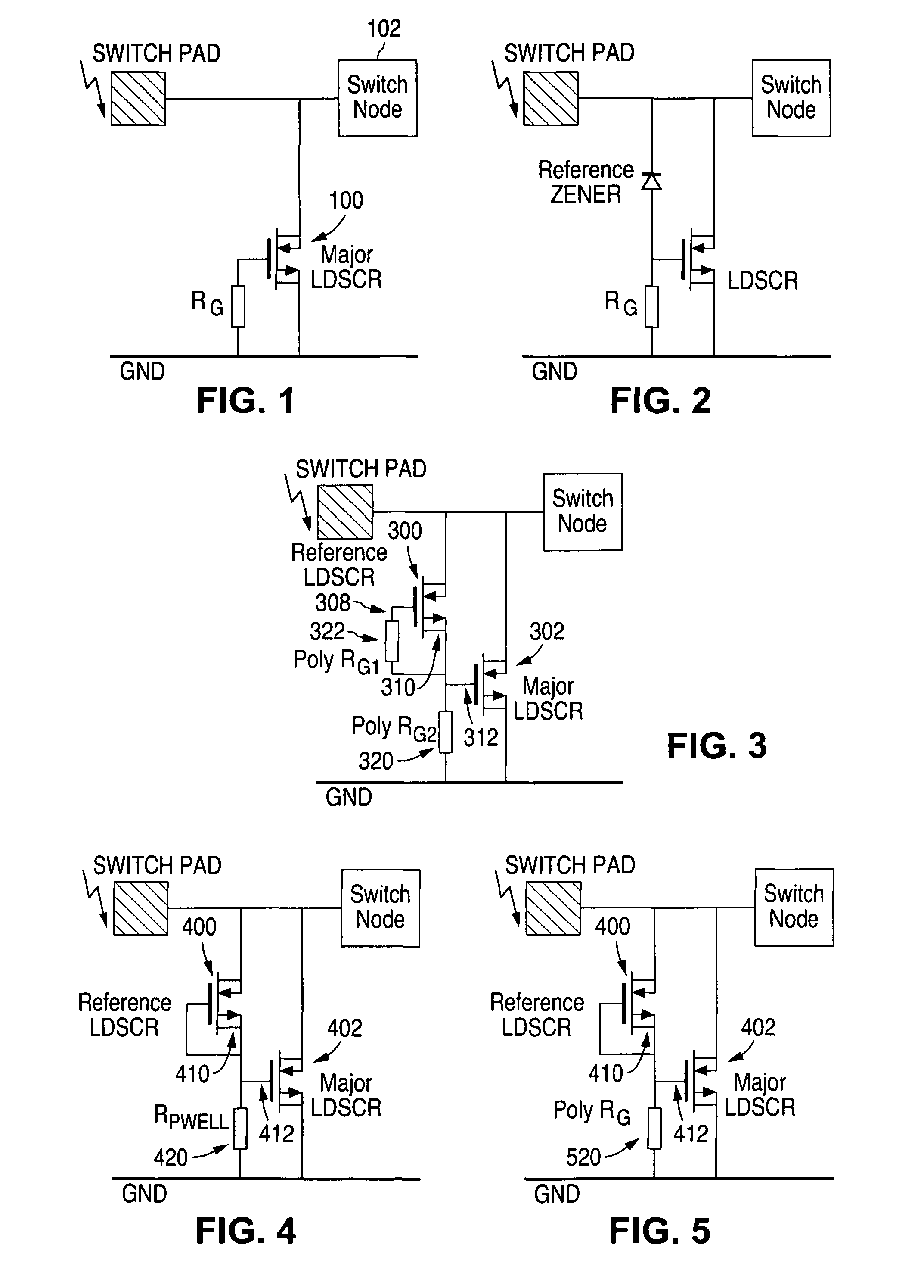
[0022]the invention is shown in FIG. 4, in which the reference LDSCR is not a separate LDSCR but constitutes one of the fingers of the LDSCR array. Thus reference LDSCR 400, which is implemented as a self triggering structure by having its gate connected to its source, is part of the same array as the major LDSCR 402. The reference LDSCR 400 again has its source 410 connected to the gate 412 of the major LDSCR 402. In this embodiment the p-well of the LDSCR acts as the resistor 420 that connects the gate 412 of the major LDSCR 402 to ground.

third embodiment

[0023]In the third embodiment shown in FIG. 5, the arrangement is essentially the same as in FIG. 4, but instead of relying on the p-well to provide the resistance for controlling the gate voltage to the major LDSCR, the FIG. 5 embodiment makes use of a separate poly resistor 520. Since the rest of the structure remains substantially the same as in FIG. 4, the same reference numerals have been used in FIG. 5 to depict similar elements as in FIG. 4.

[0024]The LDSCR arrangement thus works as follows. As the voltage increases above the reference LDSCR avalanche breakdown level, the avalanche breakdown current is realized through the gate resistor 320, 420, 520. The voltage drop on the gate resistor 320, 420, 520 creates a gate bias voltage for the major LDSCR. This results in a reduction of the snapback turn on voltage of the major LDSCR fingers, allowing them to turn on.

[0025]In order to define the avalanche breakdown voltage of the reference LDSCR, the p-well RESURF is adjusted by man...


PUM


Abstract

In an LDMOS-SCR ESD protection structure gate voltage of an ESD protection LDSCR is defined by connecting the gate to the source of a reference LDSCR. The reference LDSCR is implemented as a self-triggering device in which the snapback drain-source voltage (avalanche breakdown voltage) is controlled to be lower than that for the major LDSCR by adjusting the RESURF layer-composite overlap for the reference LDSCR to be different to that of the major LDSCR.

Description

FIELD OF THE INVENTION[0001]The invention relates to ESD devices. In particular it relates to ESD protection for high voltage and high speed devices.BACKGROUND OF THE INVENTION[0002]Electrostatic discharge (ESD) protection of high speed devices such as the protection of switch pins that extend to switch nodes with a fast rise time requirement, encounters problems when it comes to dealing with high voltages. The high voltage requirements are typically addressed by making use of an array having multiple fingers defining the protection device, to handle the high currents. However, multiple fingers invariably increase the footprint of the device, which implies a large parasitic capacitance associated with the array. This in turn is incompatible with the fast rise time requirement of the switch node.[0003]Furthermore, in the case of LDMOS-SCR devices it has been found that drain-source avalanche breakdown cannot be used to reliably turn on the device since the extended drain in such a de...

Claims


Application Information

Patent Timeline
Patent Type & Authority Patents(United States)
IPC IPC(8): H01L29/66
CPCH01L27/0266H01L29/063H01L29/7428H01L29/7436H01L29/749
Inventor VASHCHENKO, VLADISLAVHOPPER, PETER J.
Owner NAT SEMICON CORP
Why Eureka
Try Eureka