Method for manufacturing semiconductor device having buried gate

a manufacturing method and semiconductor technology, applied in the direction of semiconductor devices, basic electric elements, electrical appliances, etc., can solve the problems of -integrated semiconductor devices, -integrated drams based on 60 nm, and short channel effects, so as to reduce the number of fabrication processes

a manufacturing method and semiconductor technology, applied in the direction of semiconductor devices, basic electric elements, electrical appliances, etc., can solve the problems of -integrated semiconductor devices, -integrated drams based on 60 nm, and short channel effects, so as to reduce the number of fabrication processes

US7915121B1Active Publication Date: 2011-03-29SK HYNIX INC

Image

  • Method for manufacturing semiconductor device having buried gate
  • Method for manufacturing semiconductor device having buried gate
  • Method for manufacturing semiconductor device having buried gate

Examples


Embodiment Construction

[0028]As required, detailed embodiments of the present invention are disclosed herein. However, it is to be understood that the disclosed embodiments are merely exemplary of the invention, which may be embodied in various forms. Therefore, specific details disclosed herein are not to be interpreted as limiting, but merely as a basis for the claims and as a representative basis for teaching one skilled in the art to variously employ the present invention in virtually any appropriate manner.

[0029]Reference will now be made in detail to the embodiments of the present invention, examples of which are illustrated in the accompanying drawings. Wherever possible, the same reference numbers will be used throughout the drawings to refer to the same or like parts.

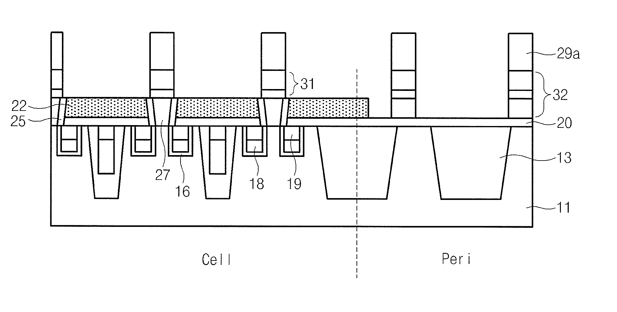
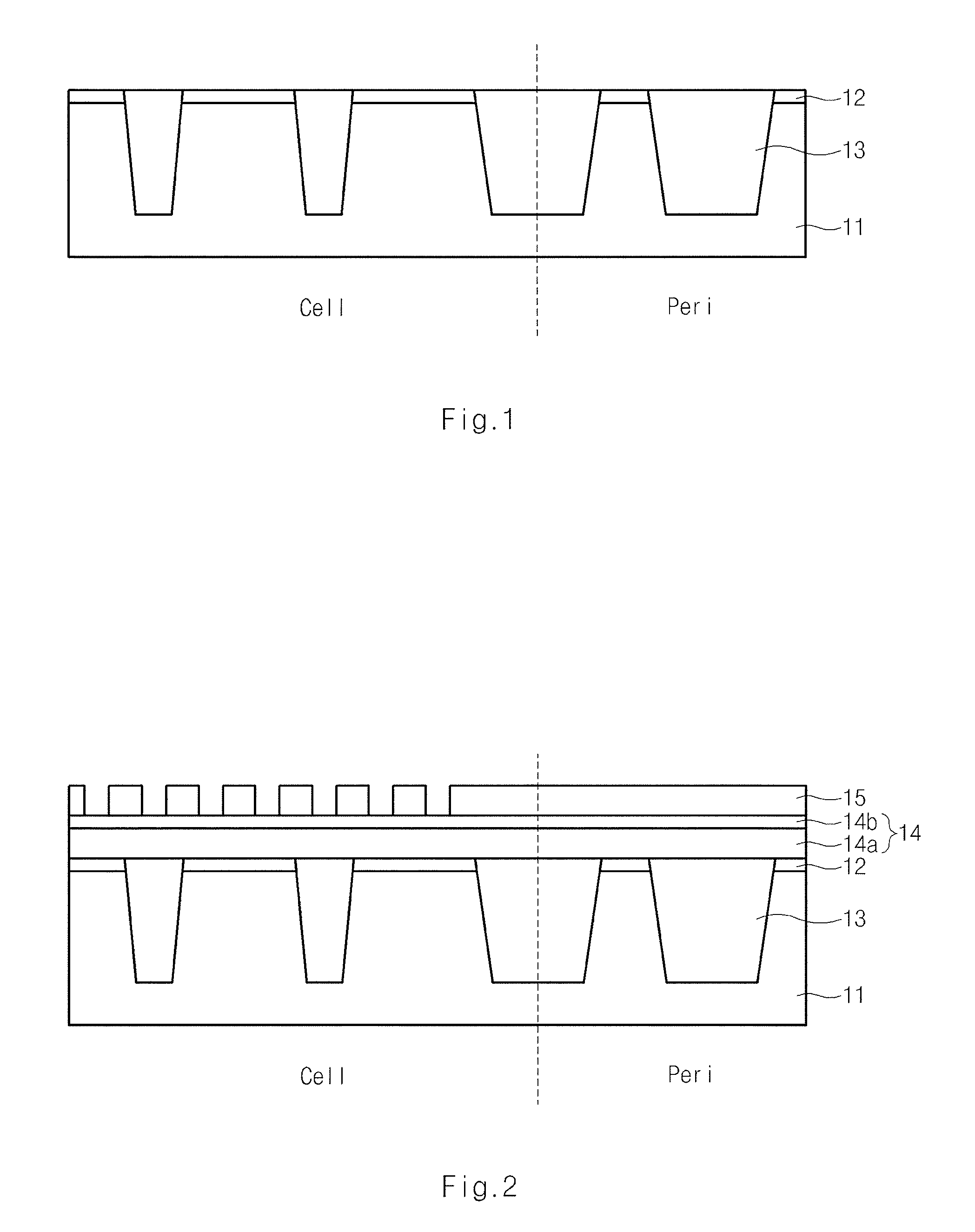
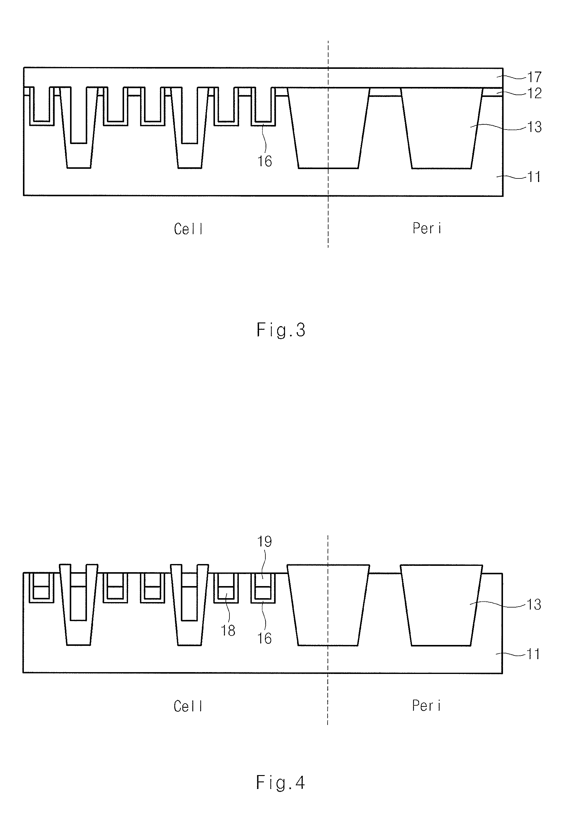
[0030]FIGS. 1 to 11 are cross-sectional views illustrating a semiconductor device including a buried gate according to an embodiment of the present invention.

[0031]Referring to FIG. 1, a pad oxide layer (not shown) and a pad nitride ...


PUM


Abstract

A method for manufacturing a semiconductor device having a buried gate is provided. A gate conductive layer is first formed in the peri region before a bit line contact is formed in the cell region, so that a fabrication process is simplified and the problem caused by a step height between the cell region and the core / peri region is not encountered.

Description

CROSS-REFERENCE TO RELATED APPLICATION[0001]The priority of Korean patent application No. 10-2009-0121765 filed on Dec. 9, 2009, the disclosure of which is hereby incorporated in its entirety by reference, is claimed.BACKGROUND OF THE INVENTION[0002]Embodiments of the present invention relate to a method for manufacturing a semiconductor device, and more particularly to a method for manufacturing a semiconductor device, such that a fabrication process of the semiconductor device having a buried gate is simplified and the number of problems caused by such a fabrication process is minimized.[0003]With the increasing integration degree of a semiconductor memory device such as a Dynamic Random Access Memory (DRAM), an area occupied by a Metal Oxide Semiconductor (MOS) transistor is gradually decreasing. As a result, a channel length of the MOS transistor is also decreasing, resulting in the occurrence of a short channel effect. Specifically, if a short channel effect occurs in an access...

Claims


Application Information

Patent Timeline
29 Mar 2011
Publication
US7915121B1
IPC
H01L21/336; H10B12/00
CPC
H01L27/10894; H01L27/10888; H01L27/10876; H01L21/823431; H10B12/053; H10B12/485; H10B12/09; H01L21/108
Inventors
KIM, YOUNG DEUK