
Semiconductor wafer and semiconductor device

a semiconductor and semiconductor technology, applied in the field of semiconductor devices, can solve problems such as peeling, safety and handling problems, shortening the process, etc., and achieve the effect of excellent low stress properties and adhesion, and low residual stress

Inactive Publication Date: 2011-03-29
SUMITOMO BAKELITE CO LTD
View PDF12 Cites 0 Cited by
  • Summary
  • Abstract
  • Description
  • Claims
  • Application Information

AI Technical Summary

Benefits of technology

[0024]The present invention can provide a semiconductor wafer using the cyclic olefin resin composition excellent in low stress properties and adhesion or the like in which the wafer breakage in a process for thinning the semiconductor wafer is suppressed and which has low residual stress. The present invention can also provide a semiconductor device using the semiconductor wafer.

Problems solved by technology

The use thereof allows simplification of a part of a pattern producing process, resulting in shortening the process.
However, since solvents such as N-methyl-2-pyrrolidone are required for the development, there are problems in safety and handling.
Since these mainly act as a permanent protective film for interlayer insulation, and exist between the circuit element and the encapsulation resin, poor adhesion of the photosensitive resin and encapsulation resin causes a problem in the generation of peelings at the interface, resulting in a lack of practicality.
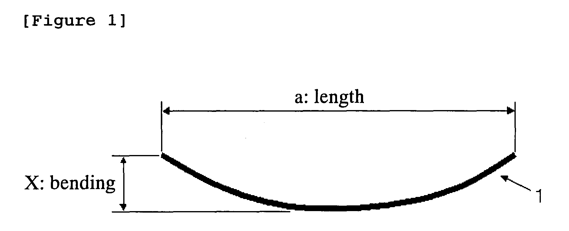
When a conventional photosensitive resin is used, bending is often generated in the large wafers, and there exists a problem in that wafers are broken in a process for grinding a backside of the wafers to make them thinner.

Method used


Image

  • Semiconductor wafer and semiconductor device
  • Semiconductor wafer and semiconductor device
  • Semiconductor wafer and semiconductor device

Examples


example 1

[0072]This example illustrates a copolymer (A-1) of 5-decyl-2-norbornene (hereinafter, referred to as “decyl norbornene”) / 5-[(2,3-epoxypropoxy)methyl]-2-norbornene (hereinafter, referred to as “glycidyl methyl ether norbornene”)=70 / 30.

[0073]All glassware was dried at 60° C. under a 0.1 torr vacuum for 18 hours. The glassware was then transferred into a glovebox and attached thereto. After ethyl acetate (917 g), cyclohexane (917 g), decyl norbornene (192 g, 0.82 mol), and glycidyl methyl ether norbornene (62 g, 0.35 mol) were added into a reaction flask, the reaction flask was taken out from the glovebox, and dry nitrogen gas was introduced into the reaction flask.

[0074]The reaction medium was degassed by passing a stream of nitrogen gas through the solution for 30 minutes. Inside the glovebox, a nickel catalyst, i.e., bis(toluene)bis(perfluorophenyl) nickel (9.36 g, 19.5 mmol), was dissolved in 15 ml of toluene, and taken up in a 25 mL syringe. The syringe was taken out from the glo...

example 2

[0092]The backside of the wafer produced in the same manner as in Example 1 and having a thickness of 725 μm was ground to 200 μm. However, breaking and cracking or the like did not occur, and a thin wafer was obtained. Then, the bending of this wafer measured by the surface roughness meter was 370 μm. The stress calculated was 5 MPa.

example 3

[0093]A terpolymer (A-2) of decyl norbornene / glycidyl methyl ether norbornene / phenethyl norbornene=55 / 30 / 15 was obtained in the same manner as in Example 1 except that decyl norbornene (129 g, 0.55 mol) and glycidyl methyl ether norbornene (177 g, 0.30 mol) and 5-(2-phenylethyl)-2-norbornene (hereinafter, referred to as “phenethyl norbornene”) (29.7 g, 0.15 mol) were used in place of decyl norbornene (192 g, 0.82 mol) and glycidyl methyl ether norbornene (62 g, 0.35 mol) of Example 1. The polymerization and the reprecipitation were carried out, and 309 g (yield: 92%) of a polymer after drying was collected. The polymer obtained had a molecular weight by GPC Mw=30000, Mn=68000, Mw / Mn=2.3. Polymer composition by H-NMR 54 mole % decyl norbornene; 31 mole % glycidyl methyl ether norbornene; and 15 mole % phenethyl norbornene.

[0094]Evaluation was made in the same manner as in Example 1.

[0095]The solder reflow resistance test and the operation confirmation of the semiconductor device were...


PUM

PropertyMeasurementUnit
thicknessaaaaaaaaaa
thicknessaaaaaaaaaa
thicknessaaaaaaaaaa

Abstract

Disclosed is a semiconductor wafer which is characterized in that a resin layer composed of a resin composition containing a cyclic olefin resin (A) having an epoxy group and a photoacid generator (B) is arranged on a surface on which a circuit element is formed, and the residual stress of the resin layer after curing is 1-20 MPa. Also disclosed is a semiconductor device comprising such a semiconductor wafer.

Description

TECHNICAL FIELD[0001]The present invention relates to a semiconductor wafer using a resin composition which is excellent in low stress properties and adhesion or the like, and to a semiconductor device produced using the semiconductor wafer.BACKGROUND ART[0002]A polyimide resin having excellent heat resistance, electrical properties, mechanical properties or the like has been used for a surface protective film and interlayer insulating film of a semiconductor element. However, improvement of properties such as thermal cycle resistance and thermal shock resistance has been required due to high integration and growth in size of the semiconductor element, thickness reduction and miniaturization of an encapsulation resin package, and shift to surface mounting by solder reflow in recent years, and a polyimide resin having higher performance has been required.[0003]On the other hand, attention has been focused on a technique for imparting photosensitivity to the polyimide resin itself. Ex...

Claims


Application Information

Patent Timeline
Patent Type & Authority Patents(United States)
IPC IPC(8): C07C1/00
CPCC08G59/3218G03F7/0382H01L23/293H01L23/3171H01L2924/0002H01L2924/00H01L23/29
Inventor KUSUNOKI, JUNYAHIRANO, TAKASHI
Owner SUMITOMO BAKELITE CO LTD
Learn More