Semiconductor device and electronic device

a semiconductor device and electronic device technology, applied in the field of semiconductor devices, can solve the problems of affecting the output of light sensors, the size of light sensors itself is further increased, and no countermeasures have been taken to protect against so as to improve the photovoltaic efficiency of photovoltaic elements, prevent damage due to electrostatic discharge, and increase the size of semiconductor devices

Inactive Publication Date: 2011-04-12
SEMICON ENERGY LAB CO LTD
View PDF36 Cites 7 Cited by
  • Summary
  • Abstract
  • Description
  • Claims
  • Application Information

AI Technical Summary

Benefits of technology

[0010]In view of the above problems, the present invention has the objective of preventing damage due to electrostatic discharge in a semiconductor device that functions as a light sensor. In addition, the present invention also has an objective of preventing damage due to electrostatic discharge without any increase in the size of the semiconductor device.
[0011]The present invention is a semiconductor device that can function as a light sensor and has a photovoltaic element and a circuit to which is input the output of the photovoltaic element. The present invention is used to prevent the occurrence of damage due to electrostatic discharge in a light sensor by provision of a portion in which damage due to electrostatic discharge occurs more readily than in a portion that functions substantially as a light sensor.
[0014]By the conductive film being provided so as to overlap with the circuit with an insulating film interposed therebetween, damage due to electrostatic discharge can be prevented without any increase in the size of the semiconductor device.
[0015]Furthermore, by a reflective film being used for the conductive film, the conductive film can be formed so as to overlap with the photovoltaic layer of the photovoltaic element. In this case, the conductive film functions as a reflective plate. As a consequence, because light passing through the photovoltaic layer can be reflected by the conductive film, the photovoltaic efficiency of the photovoltaic element can be improved.
[0016]In the present invention, by use of a conductive film, which is a means that has a simple structure, the occurrence of damage due to electrostatic discharge in a semiconductor device that has a photovoltaic element can be prevented.

Problems solved by technology

However, in conventional light sensors, no countermeasures have been taken to protect against damage due to electrostatic discharge.
Furthermore, problems arise in that the output of the light sensor is affected, the size of the light sensor itself is further increased, and the like with provision of a protective circuit.

Method used


Image

  • Semiconductor device and electronic device
  • Semiconductor device and electronic device
  • Semiconductor device and electronic device

Examples


embodiment mode 1

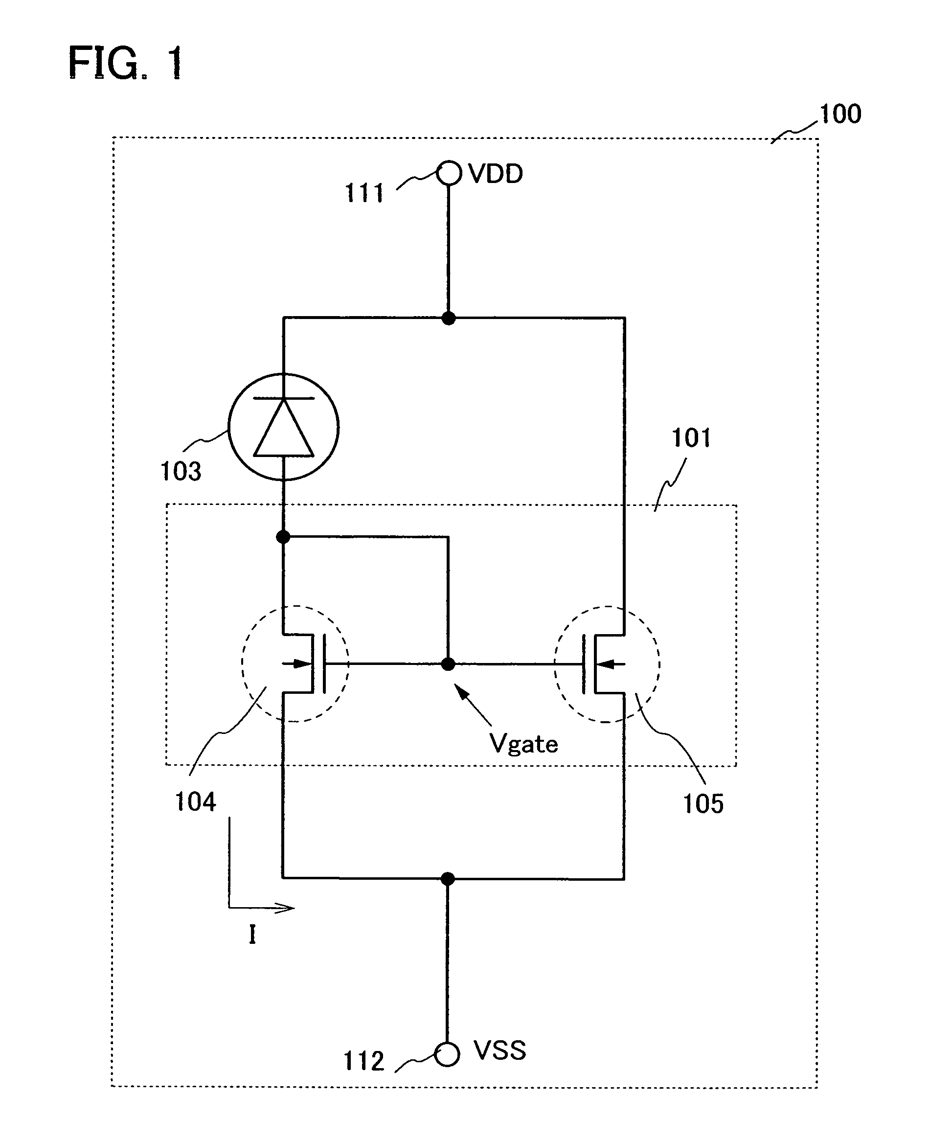
[0040]Using FIG. 1, a semiconductor device of the present invention will be described. FIG. 1 is a schematic diagram illustrating an example of a structure of a semiconductor device of the present invention. In the present embodiment mode, an example of a semiconductor device that has a photodiode used as a photovoltaic element and a current mirror circuit used as a circuit that is connected to the photovoltaic element is described.

[0041]As shown in FIG. 1, a semiconductor device 100 of the present embodiment mode has a photodiode 103 and a current mirror circuit 101 that is electrically connected to the photodiode 103. The current mirror circuit 101 is a circuit that is used to amplify the output of the photodiode 103 and is formed of a transistor 104 on the reference side and a transistor 105 on the output side. In FIG. 1, the transistor 104 and the transistor 105 are set to be n-channel transistors. Both the transistor on the output side of the current mirror circuit and the tran...

embodiment mode 2

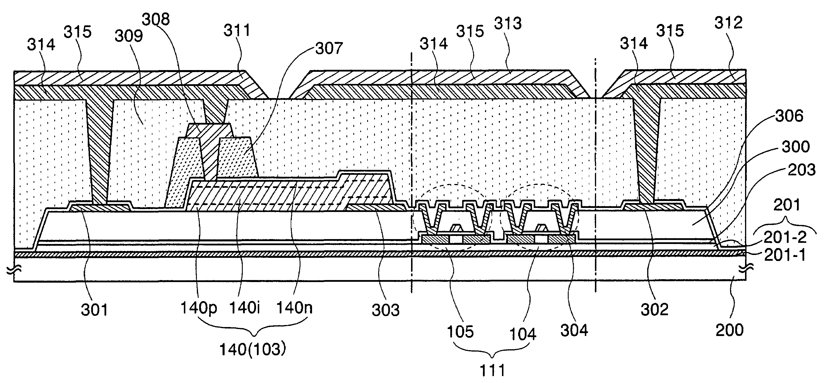
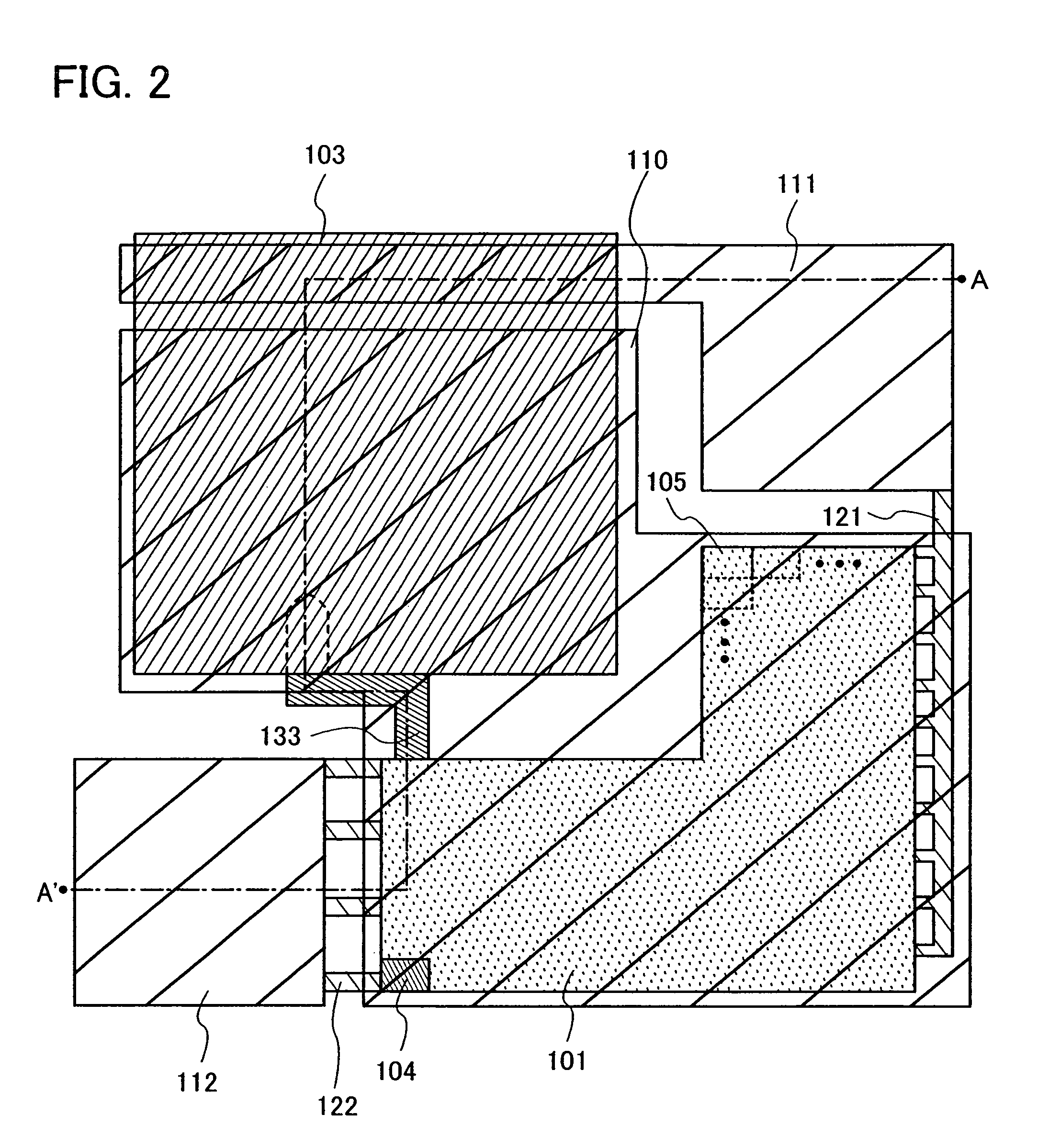
[0094]In the present embodiment mode, another example of a structure of the semiconductor device 100 that is shown in FIG. 1 will be described. FIG. 8 is a diagram used to describe the structure of a cross section of the semiconductor device 100. FIG. 9 is a plane-view diagram used to describe an example of a layout of the semiconductor device 100.

[0095]FIG. 8, as with FIG. 3, is a cross-sectional-view diagram illustrating an example of the structure of the semiconductor device 100 when the current mirror circuit 101 is formed of top-gate n-channel TFTs. In FIG. 8, for the structure of a cross section of the current mirror circuit 101, the two transistors 104 and 105 that are provided in the current mirror circuit 101 are shown.

[0096]As shown in FIG. 8, the transistors 104 and 105 of the current mirror circuit 101 are formed over the substrate 200 with the insulating layer 201 that functions as a base film interposed between the transistors 104 and 105 and the substrate 200. In the ...

embodiment mode 3

[0114]In the present embodiment mode, another example of a structure of the semiconductor device 100 that is shown in FIG. 1 will be described. FIG. 12 is a diagram used to describe the structure of a cross section of the semiconductor device 100. FIG. 13 is a plane-view diagram used to describe an example of a layout of the semiconductor device 100 of FIG. 11.

[0115]FIG. 12, as with FIG. 3, is a cross-sectional-view diagram illustrating an example of the structure of the semiconductor device 100 when the current mirror circuit 101 is formed of top-gate n-channel TFTs. In FIG. 12, for the structure of a cross section of the current mirror circuit 101, the two transistors 104 and 105 that are provided in the current mirror circuit 101 are shown.

[0116]As shown in FIG. 12, the transistors 104 and 105 of the current mirror circuit 101 are formed over the substrate 200 with the insulating layer 201 that functions as a base film interposed between the transistors 104 and 105 and the substr...


PUM


Abstract

The present invention has a photodiode and a circuit used to amplify the output of the photodiode. Two terminals are formed over the photodiode and circuit with an insulating layer interposed therebetween, and a dummy electrode with a larger area than that of either of the two terminals is formed thereover, adjacent to the two terminals. The dummy electrode is not connected to the photodiode or to the circuit of the semiconductor device. Because the dummy electrode has a wide area, damage due to electrostatic discharge occurs in the dummy electrode more easily than in the two terminals; thus, damage due to electrostatic discharge can be prevented from occurring in the semiconductor device.

Description

BACKGROUND OF THE INVENTION[0001]1. Field of the Invention[0002]The present invention relates to a semiconductor device that has a photovoltaic element.[0003]2. Description of the Related Art[0004]There are many known photovoltaic devices used in the detection of electromagnetic waves, in general, for example, an object, generally called a light sensor, that is sensitive to light from the ultraviolet region to the infrared region of the electromagnetic spectrum. Out of these light sensors, one that has sensitivity in the visible light region, wavelength in the range from 400 nm to 700 nm, is called a visible light sensor, in particular, and visible light sensors are being used in many different kinds of devices for brightness adjustment, on / off control, and the like that are needed in a person's living environment.[0005]In particular, in a display device, the brightness of ambient light around the display device is detected, and the luminance of the display is adjusted. Because the ...

Claims


Application Information

Patent Timeline
Patent Type & Authority Patents(United States)
IPC IPC(8): H01L31/0232
CPCH01L23/60H01L27/14609H01L31/02019H01L27/0248H01L27/14643H01L2924/0002H01L2924/00H01L27/146H01L31/10
Inventor HIROSE, ATSUSHISHISHIDO, HIDEAKI
Owner SEMICON ENERGY LAB CO LTD
Why Eureka
Try Eureka