Bonding method and method of manufacturing a display device

a display device and bonding method technology, applied in the direction of identification means, instruments, controlling lamination, etc., can solve the problems of air bubbles and foreign objects trapped during bonding, difficult to confirm the location of a defect in the touch panel, and inability to tell whether

Inactive Publication Date: 2011-04-19
DAWNCREST IP LLC
View PDF8 Cites 22 Cited by
  • Summary
  • Abstract
  • Description
  • Claims
  • Application Information

AI Technical Summary

Benefits of technology

[0010]The present invention has been made in view of the above-mentioned problems, and therefore has an object to provide a method that checks for foreign objects, air bubbles and other defects in the adhesive layer alone by discriminating them from defects in the transparent cover plate or the touch panel and, in the case of a photo-curing transparent adhesive is employed for bonding, that prevents a curing reaction to the check in the adhesive.
[0013]When a photo-curing transparent adhesive is employed as the transparent adhesive layer, the first step is a step of filling a gap between the transparent member and the plate-like member with the transparent adhesive, and a state of the transparent adhesive is checked in the visual check step by casting light having a wavelength that does not cause a curing reaction in the transparent adhesive from a side of the transparent adhesive, and the method further includes the step of curing the transparent adhesive by casting light having a wavelength that causes a curing reaction in the transparent adhesive from the transparent member side. Also, when a photo-curing transparent adhesive is employed as the transparent adhesive layer, the first step is a step of filling a gap between the transparent member and the plate-like member with the transparent adhesive, and a state of the transparent adhesive is checked in the visual check step by casting light containing a wavelength that causes a curing reaction in the transparent adhesive, for a period of time short enough to prevent starting the curing, from a side of the transparent adhesive, and the method further includes the step of curing the transparent adhesive by casting light having a wavelength that causes a curing reaction in the transparent adhesive from the transparent member side. According to those methods where the adhesive is not cured in the visual check step, if it is judged in this step that the adhesive contains air bubbles or foreign objects, the adhesive can be readily removed for re-bonding, and the transparent member and the plate-like member do not have to be discarded. If the item being checked is judged in this step as non-defective, on the other hand, the item can be irradiated with light under a condition that causes a curing reaction in the adhesive.
[0016]Such methods make it possible to check for air bubbles, foreign objects, and the like in the transparent adhesive with the use of light cast from a side of the transparent adhesive and having a wavelength that does not start a curing reaction and, for a defective item, to immediately repair the item that is being checked if an anomaly is found (by removing the transparent adhesive and applying a new coat of the transparent adhesive to fill the gap between the transparent plate and the plate-like member) before conducting an visual check again and, for a non-defective item, to irradiate the photo-curing adhesive with light of a wavelength that causes a curing reaction, thereby bonding the transparent plate and the plate-like member together.

Problems solved by technology

Air bubbles and foreign objects trapped during bonding are a serious issue common to all of various methods of bonding a liquid crystal display to a touch panel or a transparent cover plate that have been proposed.
Although whether air bubbles and foreign objects are being trapped is checked by casting light from the screen side of the transparent cover plate or of the touch panel after bonding in the case of a transparent adhesive sheet, or before curing in the case of a transparent adhesive, there are following problems.
The check may detect a foreign object but cannot tell whether the foreign object is in the bonded touch panel or transparent cover plate or in the bonded adhesive layer.
It is very difficult to confirm the location of a defect in the touch panel or the transparent cover plate before conducting the post-bonding check.
Also, in the case of a photo-curing transparent adhesive, especially a visible-light curable adhesive, the light cast for the check accelerates the curing of the adhesive to a point that makes it difficult to peel when a defect is found, unless the check is finished quickly.

Method used


Image

  • Bonding method and method of manufacturing a display device
  • Bonding method and method of manufacturing a display device

Examples


embodiment 1

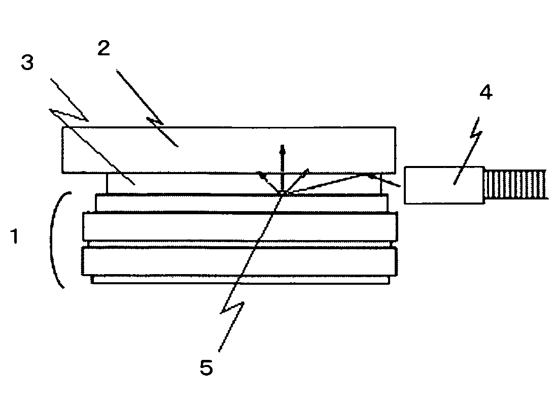
[0026]An embodiment of the present invention is described below with reference to one of the accompanying drawings. FIG. 1 is a side view showing a visual check step of a bonding method according to this embodiment. A liquid crystal display 1 and a transparent member in the form of a cover plate 2 are bonded together with a transparent adhesive sheet 3. The liquid crystal display 1 is a TFT liquid crystal display. TFT elements are formed on one of two transparent substrates each of which is made of glass and has a thickness of 0.3 mm. Formed on the other opposite transparent substrate is a color filter. Between those two transparent substrates, a TN liquid crystal is oriented along orientation films, which are formed on surfaces of the transparent substrates. A polarizing plate is attached to each transparent substrate. The transparent cover plate 2 is an acrylic plate with a thickness of 1.5 mm. A side of the transparent cover plate 2 opposite to the displaying side is painted blac...

embodiment 2

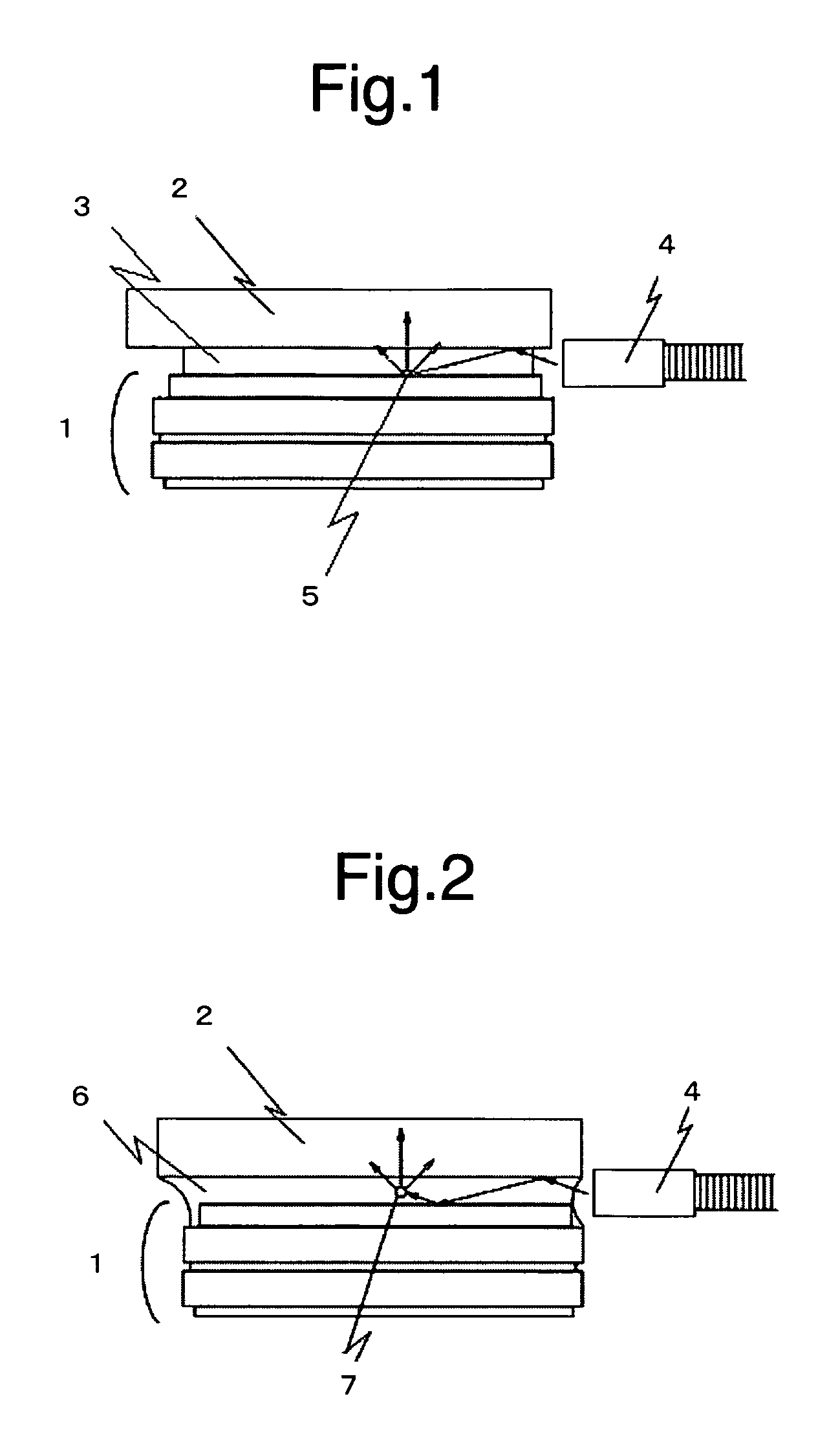
[0028]An embodiment of the present invention is described below with reference to one of the accompanying drawings. FIG. 2 is a side view showing a visual check step of a bonding method according to this embodiment. Between a liquid crystal display 1 and a transparent member or cover plate 2, a transparent adhesive 6 which is not cured yet is filled. The liquid crystal display 1 is a TFT liquid crystal display. TFT elements are formed on one of two transparent substrates each of which is made of glass and has a thickness of 0.3 mm. Formed on the other opposite transparent substrate is a color filter. Between those two transparent substrates, a TN liquid crystal is oriented along orientation films, which are formed on the surfaces of the transparent substrates. A polarizing plate is attached to each transparent substrate. The transparent cover plate 2 is an acrylic plate with a thickness of 1.5 mm. A side of the transparent cover plate 2 opposite to the displaying side is painted bla...


PUM

PropertyMeasurementUnit
thicknessaaaaaaaaaa
wavelengthaaaaaaaaaa
thicknessaaaaaaaaaa

Abstract

Air bubbles or foreign objects in a transparent adhesive layer that bonds a transparent plate and a plate-like member together in full-surface contact are detected without fail. For the detection, an optical fiber or the like is used to irradiate the adhesive layer with light from a side, the cast light is guided through the adhesive layer, and a state of the adhesive layer is checked with the guided light. A check that discriminates defects in the adhesive layer from defects in the bonded transparent plate is thus made possible.

Description

CROSS-REFERENCE TO RELATED APPLICATION[0001]This application is a U.S. national stage application of International Application No. PCT / JP2006 / 323643, filed Nov. 28, 2006, claiming a priority date of Nov. 30, 2005, and published in a non-English language.BACKGROUND OF THE INVENTION[0002]1. Field of the Invention[0003]The present invention relates to a method of bonding a transparent substrate and a substrate together with a liquid adhesive in a manner that brings the two into full-surface contact with each other. For example, the present invention relates to bonding a transparent cover plate of a cellular phone or other similar devices to a flat display such as a liquid crystal display device, a plasma display, an organic EL display, an inorganic EL display, or an FED, or bonding a touch panel to a flat display.[0004]2. Description of the Related Art[0005]Conventionally, a general method to place a transparent touch panel on a display device has been to fix the transparent touch pane...

Claims


Application Information

Patent Timeline
Patent Type & Authority Patents(United States)
IPC IPC(8): B32B41/00
CPCG01N21/958G01N21/8422G02F1/1333G09F9/00
Inventor MATSUHIRA, TSUTOMU
Owner DAWNCREST IP LLC
Why Eureka
Try Eureka