Circuit device and manufacturing method thereof

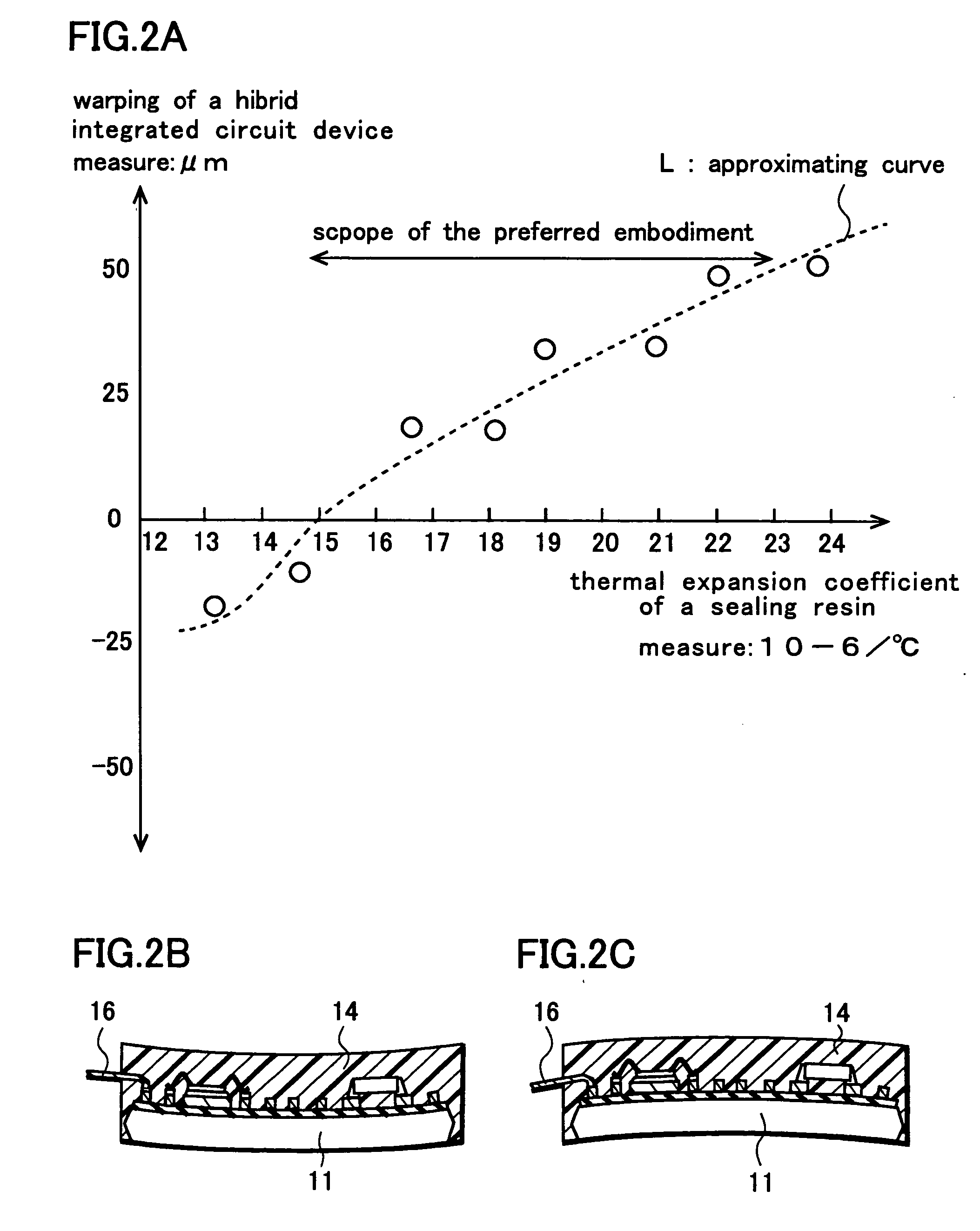
a technology of circuit device and manufacturing method, which is applied in the direction of enlarged heating surface vessel, semiconductor/solid-state device details, and gathered refuse, etc., can solve the problems of substrate b>101/b> being warped, and unable to meet the expansion and shrinkage of the substrate. , to achieve the effect of reducing the shrinkage on curing, reducing the shrinkage caused by sealing

Inactive Publication Date: 2006-03-30
SANYO ELECTRIC CO LTD +1
View PDF24 Cites 22 Cited by
  • Summary
  • Abstract
  • Description
  • Claims
  • Application Information

AI Technical Summary

Benefits of technology

[0013] Furthermore, a method for manufacturing a circuit device of the present invention includes: forming an electrical circuit on a surface of a circuit board, the electrical circuit including a conductive pattern and circuit elements; covering at least the surface of the circuit board with a sealing resin having a filler mixed therein so as to cover the circuit elements; curing the sealing resin in a manner that the circuit board is curved toward a rear surface thereof by heating the sealing resin; and allowing any of the sealing resin and the rear surface of the circuit board to come into contact with a surface of a radiator in a manner that curve of the circuit board is reduced.
[0014] Furthermore, a method for manufacturing a circuit device of the present invention includes: preparing a substrate made of any of aluminum and copper, in which a conductive pattern mainly made of copper is formed; mounting circuit elements on the substrate; and forming a resin by transfer molding so as to substantially cover at least a surface of the substrate. In the method, a thermal expansion coefficient of the resin having a filler mixed therein is selected within a range of 15×10−6 / ° C. to 23×10−6 / ° C. so as to suppress shrinkage on curing of the resin in the molding and to form a rear surface of the substrate, after the resin is cured, to be slightly convex downward.
[0018] In order to suppress this warping, in the present application, the thermal expansion coefficient of the resin is selected to be substantially the same as that of the aluminum substrate. Moreover, in order to suppress the shrinkage, a filler is mixed in the resin by about 80% thereof. This filler is originally a solid and has no shrinkage on curing. Thus, shrinkage in curing of the entire sealing resin is reduced. Considering the cured resin having the filler mixed therein, the thermal expansion coefficient thereof may be within a range of about 15×10−6 / ° C. to 23×10−6 / ° C.
[0019] Specifically, the filler may be mixed to suppress the shrinkage in curing. Moreover, the thermal expansion coefficient of the cured sealing resin having the filler mixed therein may be close to that of the aluminum substrate. However, considering an amount of the shrinkage on curing, a better balance with the expansion and shrinkage of the substrate can be achieved if the thermal expansion coefficient of the sealing resin is somewhat smaller than that of the aluminum substrate.
[0020] In an embodiment of the present invention, a sealing resin which has a thermal expansion coefficient somewhat smaller than that of a circuit board and has a filler mixed therein is used. Thus, shrinkage on curing, which is caused when the sealing resin is formed, can be reduced. Therefore, peeling and the like due to the shrinkage on curing of the sealing resin can be prevented. Furthermore, warping of the entire device is also suppressed.
[0021] Furthermore, according to a method for manufacturing a circuit device of preferred embodiment of the invention, a circuit board is slightly curved toward a rear surface thereof by shrinkage on curing of a sealing resin, and the sealing resin or the circuit board can be allowed to come into contact with a radiator. Therefore, the sealing resin or the rear surface of the circuit board can be allowed to come into close contact with the radiator. Thus, a heat releasing property can be improved.

Problems solved by technology

However, the hybrid integrated circuit device 100A described above has a problem where a crack occurs in the bond 106 due to stress caused by a temperature change.
Consequently, the crack occurs in the bond 106, and a problem of a connection failure arises.
However, when the surface of the substrate 101 is entirely sealed by use of the sealing resin 109 having the thermal expansion coefficient that approximates that of the substrate 101, there arises a problem that the substrate 101 is warped by shrinkage on curing of the sealing resin 109.
Particularly, if a planar size of the substrate 101 is as large as about 6 cm×4 cm or more, this problem of warping noticeably occurs.
Moreover, there is also a problem that large warping of the entire device makes it impossible to allow the device to come into contact with a radiator such as a radiation fin.

Method used


Image

  • Circuit device and manufacturing method thereof
  • Circuit device and manufacturing method thereof
  • Circuit device and manufacturing method thereof

Examples


Embodiment Construction

[0029] Configuration of Hybrid Integrated Circuit Device 10

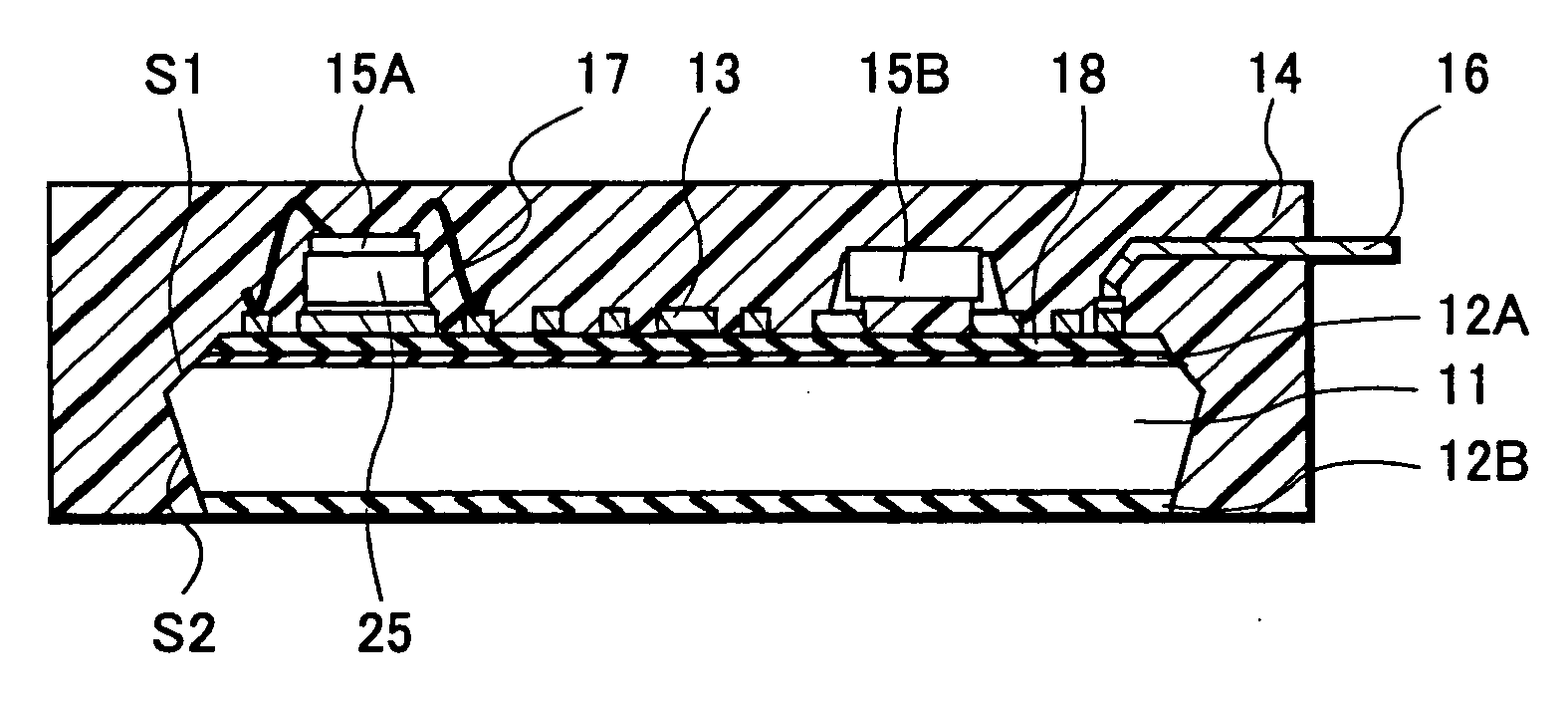
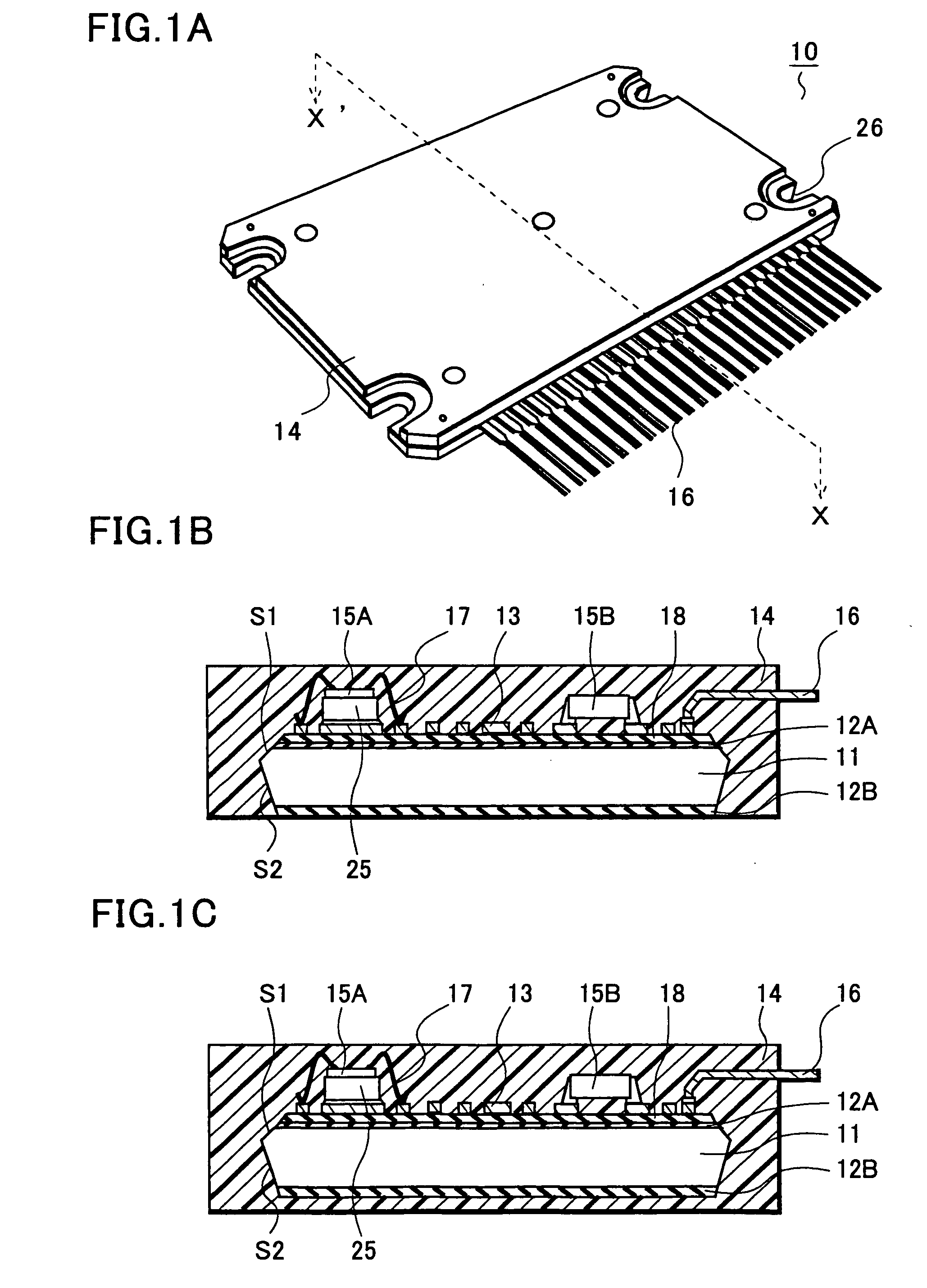
[0030] With reference to FIGS. 1A to 1C, description will be given of a configuration of a hybrid integrated circuit device 10 of preferred embodiment of the invention.

[0031] First, an insulating layer 18 is formed on a surface of a rectangular circuit board 11. Thereafter, a conductive pattern 13 having a predetermined shape is formed on a surface of the insulating layer 18. Furthermore, in predetermined spots of the conductive pattern 13, a semiconductor element 15A and a chip element 15B are electrically connected. The conductive pattern 13, the semiconductor element 15A and the chip element 15B, all of which are formed above the surface of the circuit board 11, are covered with a sealing resin 14.

[0032] The circuit board 11 is made of metal such as aluminum and copper. If aluminum is used as a material of the circuit board 11, a thermal expansion coefficient of the circuit board 11 is about 23×10−6 / ° C. A specific size...


PUM


Abstract

Warping of a hybrid integrated circuit device 10 due to shrinkage on curing of a sealing resin 14 is suppressed. The hybrid integrated circuit device 10 includes: a conductive pattern 13 provided on a surface of a circuit board 11; circuit elements 15 fixed to the conductive pattern 13; thin metal wires 17 electrically connecting the circuit elements 15 to the conductive pattern; leads 16 which are connected to the conductive pattern 13 to become output or input and extended to the outside; and a sealing resin 14 which is made of a thermosetting resin and covers the circuit board 11 by transfer molding while at least a rear surface of the circuit board is exposed. Here, a thermal expansion coefficient of the sealing resin 14 is set to be smaller than a thermal expansion coefficient of the circuit board 11. Thus, warping of the circuit board 11 in an after cure step can be prevented.

Description

[0001] Priority is claimed to Japanese Patent Application Number JP2004-288213 filed on Sep. 30, 2004, the disclosure of which is incorporated herein by reference in its entirety. BACKGROUND OF THE INVENTION [0002] 1. Field of the Invention [0003] The preferred embodiment of the invention relates to a circuit device and a manufacturing method thereof, and more particularly relates to a circuit device in which warping of a substrate is reduced, the warping being caused by heat curing of a sealing resin, and a manufacturing method thereof. [0004] 2. Description of the Related Art [0005] With reference to FIGS. 7A to 7C, a configuration of a conventional hybrid integrated circuit device 100 will be described. [0006] With reference to FIG. 7A, a configuration of a conventional hybrid integrated circuit device 100A will be described. On a surface of a rectangular substrate 101, a conductive pattern 103 is formed with an insulating layer 102 interposed therebetween. A predetermined electr...

Claims


Application Information

Patent Timeline
Patent Type & Authority Applications(United States)
IPC IPC(8): H05K5/06
CPCH01L21/565H01L2924/01006H01L23/3121H01L23/3135H01L23/49531H01L24/97H01L2224/48091H01L2224/73265H01L2224/97H01L2924/01002H01L2924/01013H01L2924/01029H01L2924/0103H01L2924/01033H01L2924/01047H01L2924/01082H01L2924/01322H01L2924/14H01L2924/19041H01L2924/19105H01L2924/30107H01L2924/3011H01L2924/3511H05K1/0271H05K1/056H05K3/284H05K3/285H05K2201/0209H05K2201/068H05K2203/0315H01L23/293H01L2924/01005H01L24/48H01L2224/85H01L2924/00014H01L2224/451H01L2924/15747H01L2924/181H01L24/45H01L2924/00H01L2224/05599H01L2924/00012A47J27/02A47J36/02A47J27/002Y10S220/912
Inventor ARAI, KAZUMASAKUBOTA, YUTAKAIGARASHI, YUSUKESAITO, HIDEFUMIMOTEGI, MASAMISAKAMOTO, NORIAKI
Owner SANYO ELECTRIC CO LTD
Why Eureka
Try Eureka