Semiconductor switching element

a switching element and semiconductor technology, applied in the field of switching elements, can solve the problems of difficult to alleviate the electric field concentration around the corner of the trench in a long direction, and achieve the effect of high voltage resistan

Active Publication Date: 2019-07-30
TOYOTA JIDOSHA KK +1
View PDF73 Cites 0 Cited by
  • Summary
  • Abstract
  • Description
  • Claims
  • Application Information

AI Technical Summary

Benefits of technology

[0006]The electric field concentration around an end (that is, the corner) of the trench in a short direction can be alleviated by providing trenches in parallel. Contrary to this, it was difficult to alleviate the electric field concentration around an end (that is, the corner) of the trench in a long direction. Thus, the disclosure herein provides a technique to improve voltage resistance of a switching element by suppressing an electric field concentration around an end of a trench in a long direction.
[0009]When this switching element turns off, a depletion layer expands from an interface between the body region and the second semiconductor region. Further, a depletion layer expands from an interface between the bottom region and the second semiconductor region (that is, from the lower surface of the bottom region) as well. The second semiconductor region is depleted by these depletion layers. Further, the depletion layer expanding from the interface between the bottom region and the second semiconductor region expands into the bottom region as well. The second bottom region extends to a lower side than the first bottom region (that is, a lower surface of the second bottom region is located on the lower side than a lower surface of the first bottom region). Due to this, an upper end of the depletion layer in the second bottom region comes to be located on the lower side than an upper end of the depletion layer in the first bottom region. Since the electric field is generated in a depleted region, in a depleted range within the second bottom region, equipotential lines are distributed on the lower side than in a depleted range within the first bottom region. Due to this, in the depleted range within the first bottom region, the equipotential lines are distributed in a state where they gradually shift upward from the second bottom region toward the end of the trench in the long direction. As a result, the curve in the equipotential lines around the corner between an end surface (side surface) of the trench in the long direction and the bottom surface of the trench is alleviated. Due to this, intervals between the equipotential lines are suppressed from becoming narrow around the corner, and an electric field concentration around the corner is suppressed. Due to this, this switching element exhibits a high voltage resistance.

Problems solved by technology

Contrary to this, it was difficult to alleviate the electric field concentration around an end (that is, the corner) of the trench in a long direction.

Method used


Image

  • Semiconductor switching element
  • Semiconductor switching element
  • Semiconductor switching element

Examples


first embodiment

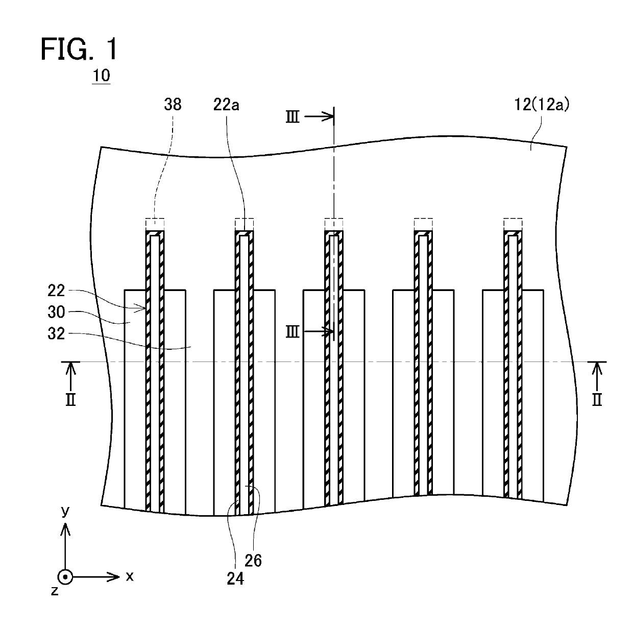
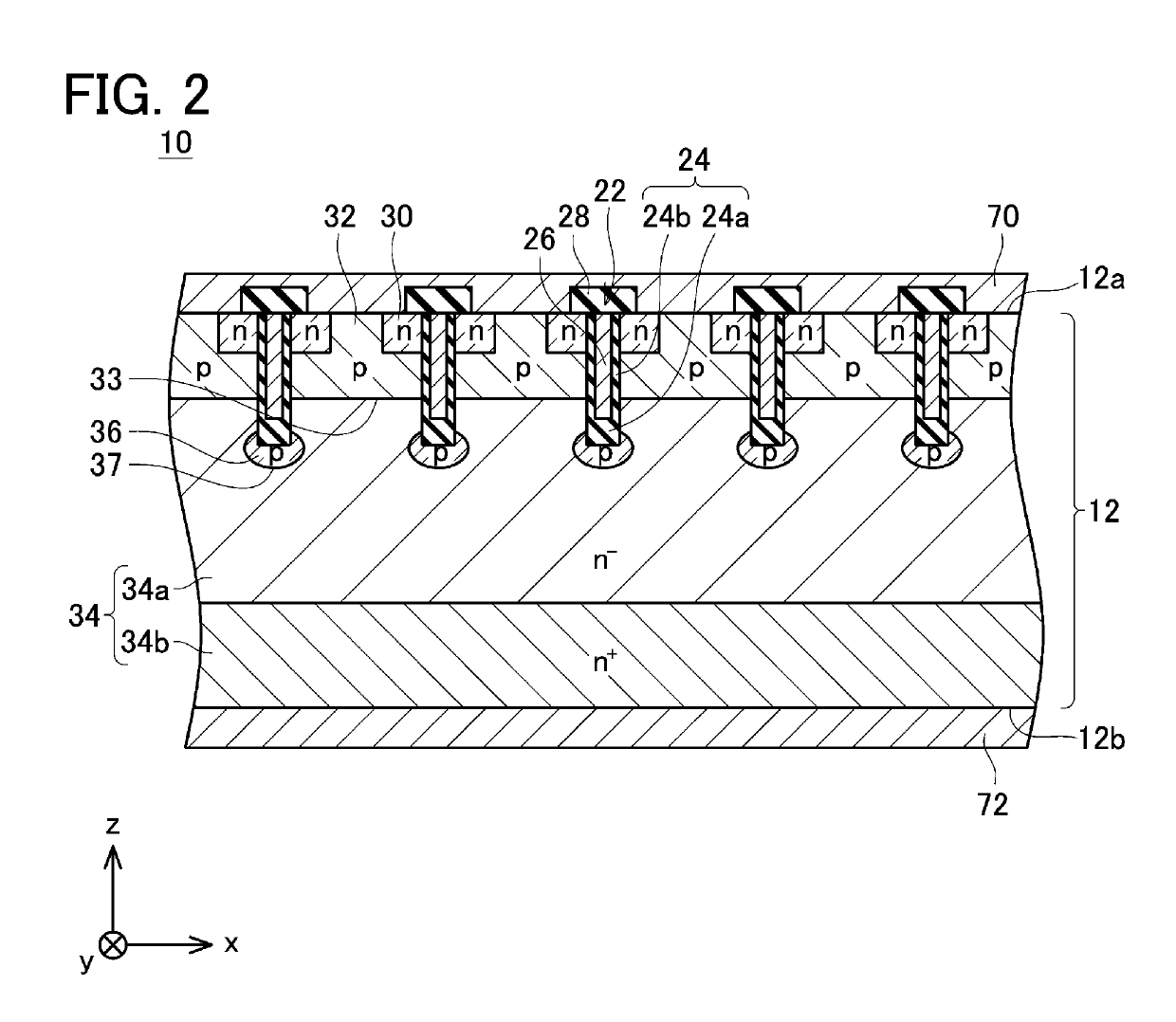
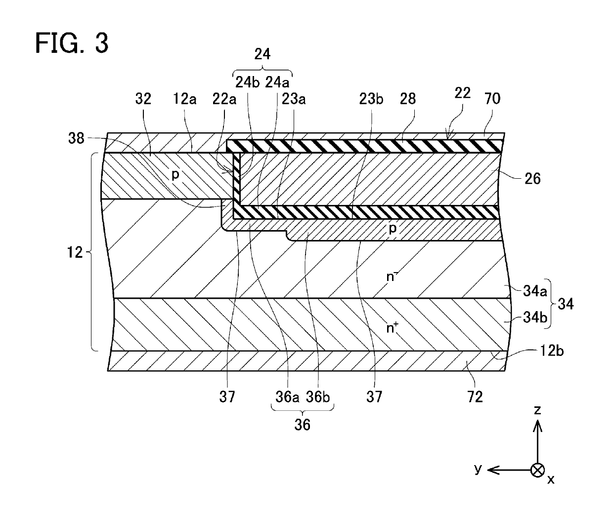
[0020]FIGS. 1 to 3 show a MOSFET (Metal-Oxide-Semiconductor Field-Effect Transistor) 10 of a first embodiment. As shown in FIGS. 2 and 3, the MOSFET 10 comprises a semiconductor substrate 12, electrodes, insulation layers, and the like. Notably, for a clearer view, FIG. 1 omits depiction of an electrode and insulation layers on an upper surface 12a of the semiconductor substrate 12. Hereinbelow, a direction parallel to the upper surface 12a of the semiconductor substrate 12 will be termed an x direction, a direction parallel to the upper surface 12a of the semiconductor substrate 12 and orthogonally crossing the x direction will be termed a y direction, and a thickness direction of the semiconductor substrate 12 will be termed a z direction. The semiconductor substrate 12 is constituted of SiC (silicon carbide).

[0021]As shown in FIG. 2, the upper surface 12a of the semiconductor substrate 12 is provided with a plurality of trenches 22. As shown in FIG. 1, each of the trenches 22 ext...

second embodiment

[0044]FIGS. 7 and 8 each show a MOSFET of a second embodiment. In the MOSFET of the second embodiment, the p-type impurity concentration of the second bottom regions 36b is higher than the p-type impurity concentration of the first bottom regions 36a. Other configurations of the MOSFET of the second embodiment are similar to those of the MOSFET 10 of the first embodiment.

[0045]As described above, in the MOSFET of the second embodiment, the p-type impurity concentration of the second bottom regions 36b is higher than the p-type impurity concentration of the first bottom regions 36a. Due to this, it is more difficult for the depletion layer to extend in the second bottom regions 36b than in the first bottom regions 36a. Due to this, as shown in FIG. 8, when the MOSFET of the second embodiment turns off, a width of the depletion layer extending into the second bottom regions 36b from the pn junctions 37 is smaller than a width of the depletion layer extending into the first bottom regi...


PUM


Abstract

A trench gate semiconductor switching element is provided. The semiconductor substrate of the element includes a second conductivity type bottom region in contact with the gate insulation layer at a bottom surface of the trench, and a first conductivity type second semiconductor region extending from a position in contact with a lower surface of the body region to a position in contact with a lower surface of the bottom region. The bottom region includes a first bottom region in contact with the gate insulation layer in a first range of the bottom surface positioned at an end in a long direction of the trench and extending from the bottom surface to a first position; and a second bottom region in contact with the gate insulation layer in a second range adjacent to the first range and extending from the bottom surface to a second position lower than the first position.

Description

TECHNICAL FIELD[0001]The present disclosure relates to a switching element.BACKGROUND ART[0002]Patent literature 1 discloses a switching element. This switching element includes a semiconductor substrate having a trench provided on its upper surface. An inner surface of the trench is covered by a gate insulation layer. A gate electrode is arranged within the trench. The gate electrode is insulated from the semiconductor substrate by the gate insulation layer. An n-type source region, a p-type body region, an n-type drift region, and a p-type bottom region (p-diffused region) are provided in the semiconductor substrate. The source region is in contact with the gate insulation layer. The body region is in contact with the gate insulation layer on a lower side of the source region. The bottom region is in contact with the gate insulation layer at a bottom surface of the trench. The drift region extends from a position being in contact with a lower surface of the body region to a positi...

Claims


Application Information

Patent Timeline
Patent Type & Authority Patents(United States)
IPC IPC(8): H01L29/08H01L29/78H01L29/06H01L29/16H01L29/36H01L21/04H01L21/265H01L29/423H01L29/66H01L29/739H01L29/10H01L29/417
CPCH01L29/7813H01L21/26513H01L21/26586H01L29/0623H01L29/0696H01L29/0865H01L29/1095H01L29/16H01L29/1608H01L29/36H01L29/41741H01L29/4236H01L29/42368H01L29/66068H01L29/66734H01L29/7397H01L21/047H01L29/66348
Inventor SAITO, JUNAOI, SACHIKOURAKAMI, YASUSHI
Owner TOYOTA JIDOSHA KK
Why Eureka
Try Eureka