Semi-finished package and method for making a package

a semi-finished package and package technology, applied in the direction of semiconductor devices, semiconductor/solid-state device details, coatings, etc., can solve the problems of increasing the thickness increasing the warpage of the first conventional semi-finished package. achieve the effect of overcoming the warpage increasing the yield rate of the package unit after cutting, and increasing the rigidity of the semi-finished packag

Active Publication Date: 2011-04-19
ADVANCED SEMICON ENG INC
View PDF3 Cites 1 Cited by
  • Summary
  • Abstract
  • Description
  • Claims
  • Application Information

AI Technical Summary

Benefits of technology

[0011]Thus, by utilizing the outer protrusions, the rigidity of the semi-finished package is increased, so as to overcome the warpage of the semi-finished package caused by different coefficients of thermal expansion of the molding compound and the carrier. Therefore, the yield rate of the package unit after cutting is increased.

Problems solved by technology

However, the coefficients of thermal expansion of the above-mentioned devices are different, so the shrinkages of the carrier 11, the molding compound 13 and the chips 12 are different after the molding process is finished and the temperature is lowered, which leads to the warpage of the first conventional semi-finished package 1, as shown in FIG. 2.
Moreover, since semiconductor packages are getting smaller and lighter nowadays, the carrier 11 and the molding compound 13 are getting thinner, and the warpage is getting more serious.
The overly warped semi-finished package 1 will cause various problems, e.g., it will stick on tables, it will be difficult to hold the package, laser marking will fail, it will be difficult to form solder balls, some solder balls will be missing, the package unit will be overly warped and coplanarity will not exist.

Method used


Image

  • Semi-finished package and method for making a package
  • Semi-finished package and method for making a package
  • Semi-finished package and method for making a package

Examples


Embodiment Construction

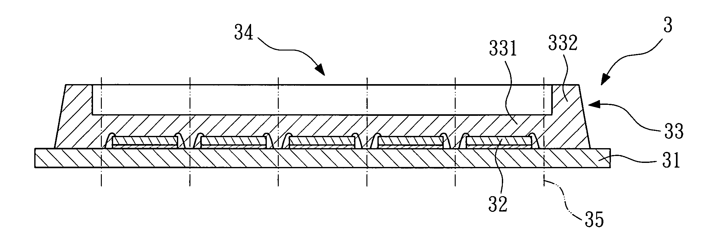
[0029]FIGS. 4 to 7 show schematic views of a method for making a package according to a first embodiment of the present invention. First, as shown in FIG. 4, a carrier 31 is provided. The carrier 31 has a plurality of chips 32 electrically connected to it. In the embodiment, the carrier 31 is a substrate; however, in other applications, the carrier 31 may be a leadframe.

[0030]As shown in FIGS. 5 and 6, at least one molding compound 33 is formed on the carrier 31 so as to encapsulate the chips 32. The molding compound 33 has a body 331 and a plurality of outer protrusions 332. The outer protrusions 332 are disposed at the periphery of the body 331, and the height of the outer protrusions 332 is greater than that of the body 331.

[0031]In the embodiment, the molding compound 33 has four outer protrusions 332 disposed at four sides of the body 331. The outer protrusions 332 define a space 34, and at least one chip 32 is disposed in the space 34. In the embodiment, all of the chips 32 ar...


PUM

PropertyMeasurementUnit
heightaaaaaaaaaa
temperatureaaaaaaaaaa
coefficients of thermal expansionaaaaaaaaaa

Abstract

The present invention relates to a semi-finished package and a method for making a package. The semi-finished package includes a carrier and at least one molding compound. The molding compound is disposed on a surface of the carrier, and has a body and a plurality of outer protrusions. The outer protrusions are disposed at the periphery of the body, and the height of the outer protrusions is greater than that of the body. Thus, by utilizing the outer protrusions, the rigidity of the semi-finished package is increased, so as to overcome the warpage of the semi-finished package caused by different coefficients of thermal expansion of the molding compound and the carrier. Therefore, the yield rate of the package unit is increased.

Description

BACKGROUND OF THE INVENTION[0001]1. Field of the Invention[0002]The present invention relates to a semi-finished package and a method for making a package, and more particularly to a semi-finished package having a molding compound with a plurality of outer protrusions and a method for making a package by cutting the semi-finished package.[0003]2. Description of the Related Art[0004]FIG. 1 shows a cross-sectional view of a first conventional semi-finished package. The first conventional semi-finished package 1 comprises a carrier 11, a plurality of chips 12 and a molding compound 13. The molding compound 13 is disposed on a surface of the carrier 11 so as to encapsulate the chips 12.[0005]The first conventional semi-finished package 1 has the following disadvantage. During a molding process, the molding compound 13 of the first conventional semi-finished package 1 is melted after heating, so as to encapsulate the chips 12. The carrier 11 and the chips 12 expand during the heating pro...

Claims


Application Information

Patent Timeline
Patent Type & Authority Patents(United States)
IPC IPC(8): H01L23/28
CPCB29C45/0025B29C45/14655B29C45/14836H01L21/561H01L21/565H01L23/3128H01L24/97B29C45/0055H01L2224/32225H01L2224/48091H01L2224/48227H01L2224/73265H01L2224/97H01L2924/15311H01L2924/1815H01L2924/3511H01L24/48H01L2924/01005H01L2924/01006H01L2924/01033H01L2224/32245H01L2224/48247H01L2924/00014H01L2224/85H01L2224/83H01L2924/00H01L2924/00012H01L2924/181H01L24/73H01L2224/45099H01L2224/45015H01L2924/207
Inventor CHENG, REN-YICHEN, KUANG-HSIUNGHSU, CHUN-HUNG
Owner ADVANCED SEMICON ENG INC
Why Eureka
Try Eureka