Method for dividing semiconductor wafer and manufacturing method for semiconductor devices

a technology of semiconductor wafers and manufacturing methods, applied in semiconductor/solid-state device manufacturing, basic electric elements, electric devices, etc., can solve the problems of small pieces of wafers jumping off, and achieve the effect of preventing the formation of comparatively small pieces of semiconductor wafers, and reducing the risk of falling o

Active Publication Date: 2011-04-19
PANASONIC CORP
View PDF17 Cites 115 Cited by
  • Summary
  • Abstract
  • Description
  • Claims
  • Application Information

AI Technical Summary

Benefits of technology

[0009]Accordingly, an object of the present invention is to solve the above-described problem and provide a method for dividing a semiconductor wafer, as well as a manufacturing method for semiconductor devices according to which a semiconductor wafer having a plurality of semiconductor devices can be divided into individual pieces. Each of the pieces is one of the above-described semiconductor devices while preventing pieces of wafer created through this dividing process from sticking to the surface of any of the semiconductor devices that have been divided into individual pieces.
[0022]According to the first aspect of the present invention, regions in approximately triangular form, which are relatively small regions, from among regions that do not become unit-device-formation-regions in the respective imaginary-divided-regions are assumed to be removal-regions to be removed, and plasma etching is carried out using a mask that has been placed so as to expose portions (regions) of the surface of the semiconductor wafer that correspond to the removal-regions, and thereby, the portions that correspond to the removal-regions in the above described semiconductor wafer can be removed and eliminated. Accordingly, the formation of comparatively small pieces in the semiconductor wafer can be prevented, and thus, the occurrence of problems caused by such pieces of the wafer, for example, problems where such pieces stick to surfaces of semiconductor devices, can be prevented reliably.
[0023]In addition, such removing processing of the removal-regions is carried out through plasma etching for dividing the semiconductor devices into individual pieces, and therefore, it is not necessary to add a separate process for removing them, and thus, an efficient process can be carried out.
[0024]According to the second aspect of the present invention, each of the removal-regions are small regions in comparison with each of the unit-device-formation-regions, such that the length dimension of segments which partition each of the removal-regions is shorter than that of the segments which partition each of the unit-device-formation-regions, and thereby, particles that relatively easily jump off can be removed reliably, by removing the removal-regions, and thus, problems such as jumping off of such pieces of the wafer can be effectively prevented.
[0025]According to the third mode, said mask is placed so as to expose the entirety of the imaginary-dividing-lines that have been arranged on the surface on the side on which the mask is placed, and thereby, the regions that are located so as to surround the unit-device-formation-regions in the semiconductor wafer and have not become either the unit-device-formation-regions or the removal-regions can be cut out along the dividing lines as individual divided pieces. As described above, the regions that are located so as to surround the unit-device-formation-regions, that is to say, the semiconductor devices, are not left as large lumps, and are left in a state where they are divided into individual pieces, and thereby, it becomes possible to smoothly expand the wafer sheet (adhesive sheet) when each of the semiconductor devices is picked up.
[0026]According to the fourth aspect of the present invention, all the regions that do not become the unit-device-formation-regions from among the imaginary-divided-regions are removed through the plasma etching as the removal-regions, and thereby, the portions other than the semiconductor devices in the semiconductor wafer can be completely removed, and thus, dividing process where no waste pieces are created can be implemented.

Problems solved by technology

In the case where the pieces of wafer are miniaturized in this manner, however, the small pieces of wafer that have been made to adhere to a wafer sheet on which the dicing process has been carried out, are caused to jump off, because of the expansion of this wafer sheet at the time when this wafer sheet is expanded.
As a result, the pieces stick to the surface of the semiconductor devices, and in some cases, a problem arises due to the pieces causing failure in the mounting of these semiconductor devices.
In addition, in some cases, the small pieces of the wafer jump off because of vibration in the wafer sheet, caused by the pick-up operation at the time when the individual semiconductor devices are picked up, in addition to when the wafer sheet is expanded.

Method used


Image

  • Method for dividing semiconductor wafer and manufacturing method for semiconductor devices
  • Method for dividing semiconductor wafer and manufacturing method for semiconductor devices
  • Method for dividing semiconductor wafer and manufacturing method for semiconductor devices

Examples


Embodiment Construction

[0050]Before the description of the present invention proceeds, it is to be noted that like parts are designated by like reference numerals throughout the accompanying drawings.

[0051]Hereinbelow, one embodiment of the present invention is described in detail with reference to the accompanying drawings.

[0052]A method for dividing a semiconductor wafer and a manufacturing method for a semiconductor device according to one embodiment of the present invention are described below. The configurations of apparatuses that are used in the method for dividing a semiconductor wafer and the manufacturing method for a semiconductor device are first described.

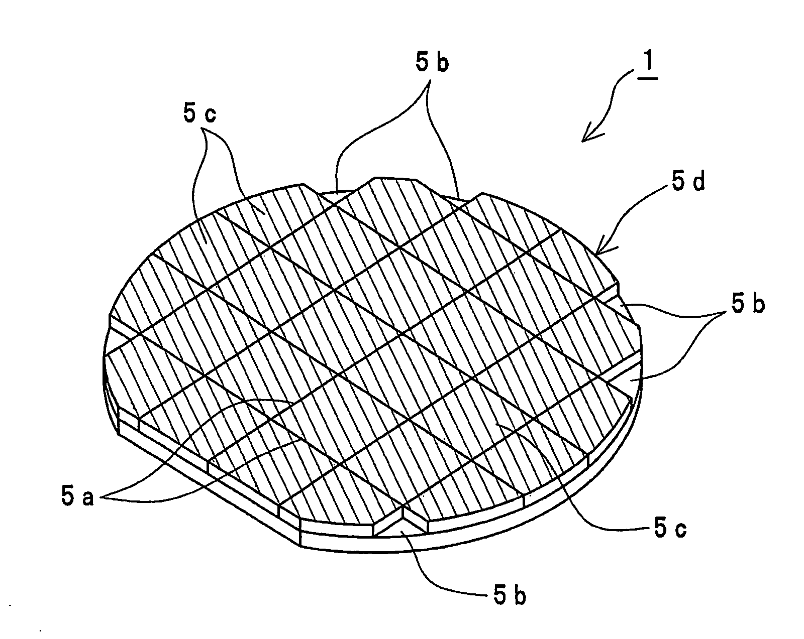
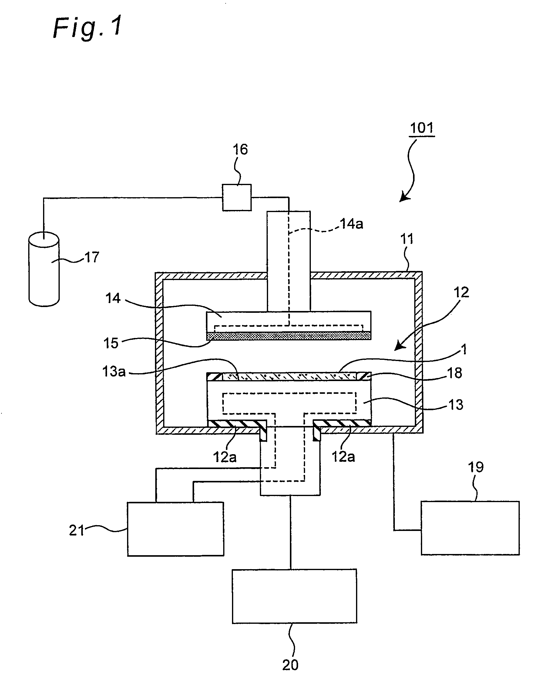
[0053]FIG. 1 is a diagram that schematically shows the configuration of a plasma processing apparatus 101, which is an example of a semiconductor wafer dividing unit in accordance with the method for dividing a semiconductor wafer of the present embodiment. This plasma processing apparatus 101 is an apparatus for performing a plasma etching ...


PUM


Abstract

In a semiconductor wafer including a plurality of imaginary-divided-regions which are partitioned by imaginary-dividing-lines that are respectively arranged in a grid-like arrangement on the semiconductor wafer and a circumferential line that is the outer periphery outline of the semiconductor wafer, a mask is placed so as to expose an entirety of surfaces of the wafer corresponding to respective removal-regions. The removal-regions are regions in approximately triangular form partitioned by the circumferential line of the wafer and the imaginary-dividing-lines. Then, plasma etching is performed on a mask placement-side surface of the wafer, by which the semiconductor wafer is divided into the individual semiconductor devices along dividing lines while portions corresponding to the removal-regions of the wafer are removed.

Description

BACKGROUND OF THE INVENTION[0001]1. Technical Field[0002]The present invention relates to a method for dividing a semiconductor wafer according to which a semiconductor wafer having a plurality of semiconductor devices is divided into individual pieces, such that each is one of the above described semiconductor devices, as well as a manufacturing method for semiconductor devices.[0003]2. Description of the Related Art[0004]Various processes for dividing a semiconductor wafer of this type, that is to say, various manners of a dicing process in semiconductor device manufacturing processes have been known. There is, for example, a method for dividing semiconductor devices that have been respectively formed on a semiconductor wafer into individual semiconductor devices by mechanically cutting the semiconductor wafer along dividing lines using a disc-shaped cutter that uses diamond or the materials and is referred to as a dicer (see, for example, Japanese Unexamined Patent Publication No...

Claims


Application Information

Patent Timeline
Patent Type & Authority Patents(United States)
IPC IPC(8): H01L21/78H01L21/308
CPCH01L21/78
Inventor HAJI, HIROSHIARITA, KIYOSHINAKAGAWA, AKIRANODA, KAZUHIRO
Owner PANASONIC CORP
Why Eureka
Try Eureka