Check patentability & draft patents in minutes with Patsnap Eureka AI!

Reflow process evaluation device and reflow process evaluation method

a technology of process evaluation and process, applied in the direction of instruments, semiconductor/solid-state device details, apparatus for force/torque/work measurement, etc., can solve problems such as securing the reliability of products

Inactive Publication Date: 2011-05-17
FUJITSU LTD
View PDF3 Cites 1 Cited by
  • Summary
  • Abstract
  • Description
  • Claims
  • Application Information

AI Technical Summary

Benefits of technology

The present invention provides a device for evaluating the quality of a reflow process used to join chips and substrates with solder. The device calculates the average principal stress on the joint area and uses a relational expression to determine the likelihood of rupture occurrence. This allows for better control and optimization of the reflow process.

Problems solved by technology

Owing to a thermal stress when soldering the LSI chip with the substrate, a joined solder portion on the side of the wiring layer of the LSI chip may be stripped (e.g., near the wiring layer in the enlarged view of FIG. 8), resulting in a significant problem in securing the reliability of the product.

Method used


Image

  • Reflow process evaluation device and reflow process evaluation method
  • Reflow process evaluation device and reflow process evaluation method
  • Reflow process evaluation device and reflow process evaluation method

Examples


Embodiment Construction

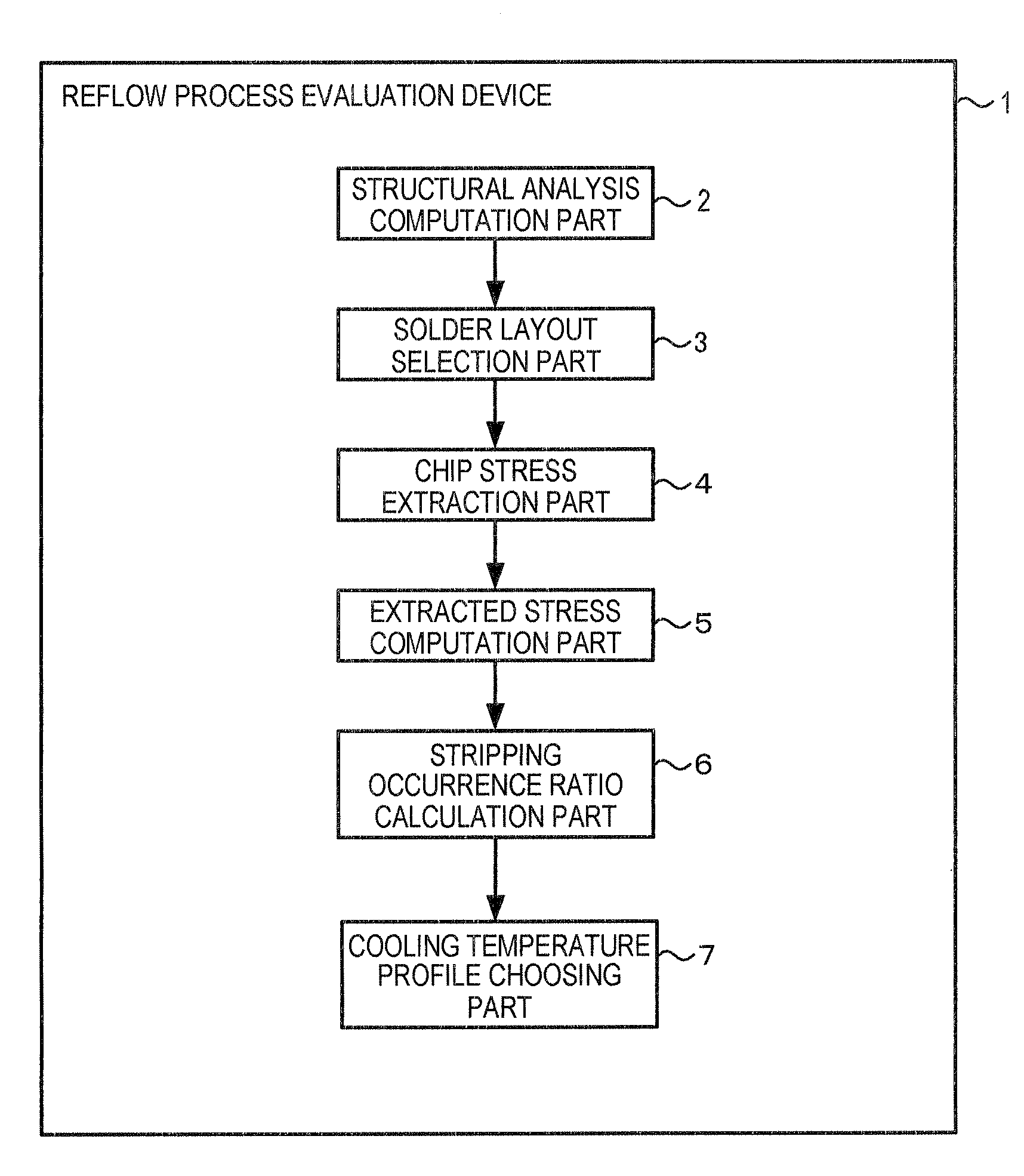
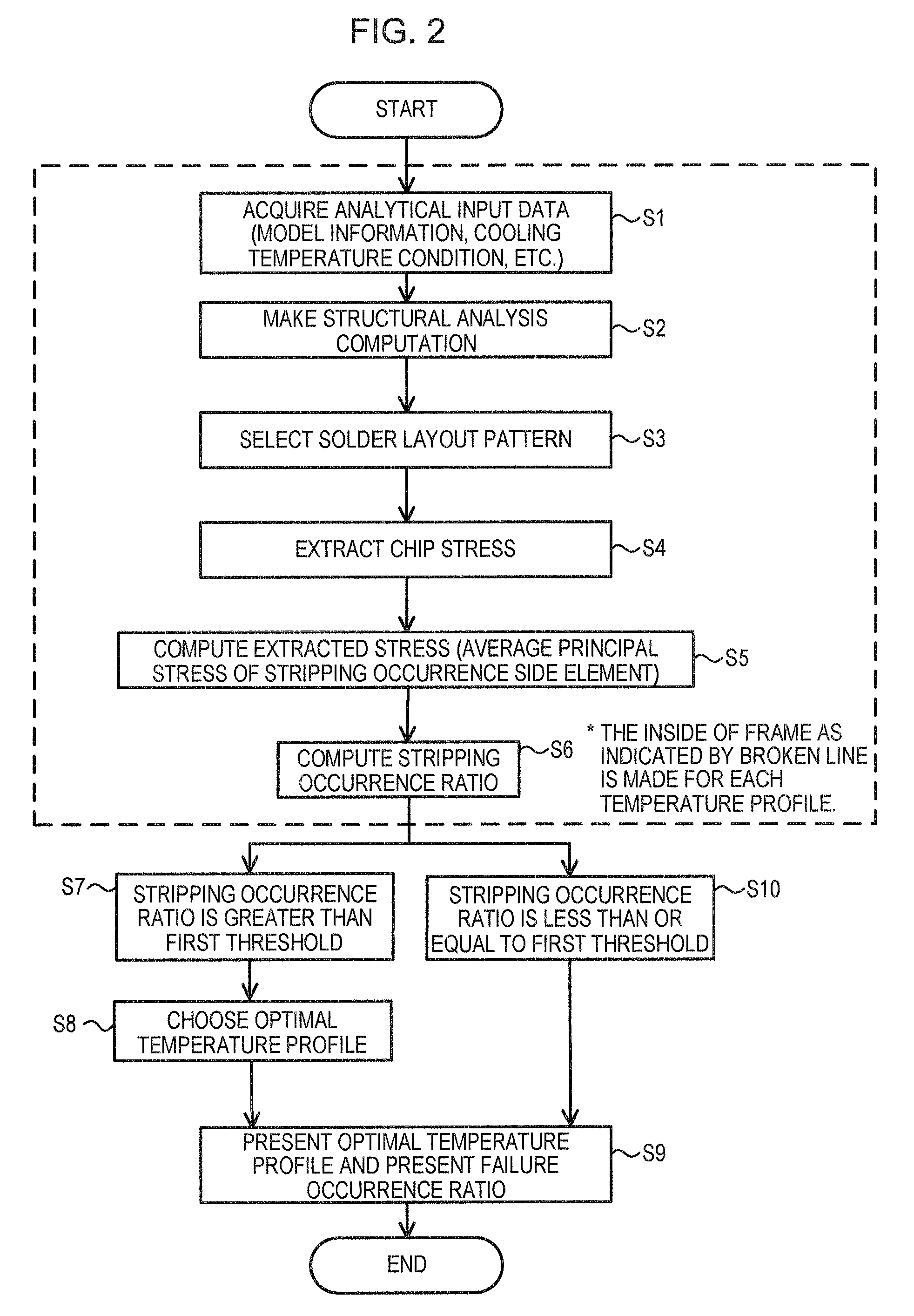
[0023]The embodiments of the present invention will be described below with reference to the drawings. First of all, a reflow process evaluation device according to an embodiment is shown in FIG. 1.

[0024]The reflow process evaluation device 1 according to an embodiment comprises a structural analysis computation part 2, a solder layout selection part 3, a chip stress extraction part 4, an extracted stress computation part 5, a stripping occurrence ratio calculation part 6, and a cooling temperature profile choosing part 7. The reflow process evaluation device 1 is a computer having the hardware resources such as a CPU, a memory, a hard disk drive, and an input / output unit Each of the above-mentioned parts is realized in cooperation with each hardware resource and software provided for the reflow process evaluation device 1.

[0025]The structural analysis computation part 2 computes the principal stress acting on the overall LSI chip in consideration of the model information or cooling...


PUM

PropertyMeasurementUnit
temperatureaaaaaaaaaa

Abstract

A reflow process evaluation device includes, a stress calculation part for calculating an average principal stress acting on a joint portion, wherein a principal stress occurs when a chip and a substrate are joined by solder with a reflow method and a rupture occurrence ratio computation part for computing an occurrence ratio at which the joint portion ruptures based on a relational expression between the occurrence ratio and the average principal stress acting on the joint portion and the average principal stress calculated by the stress calculation part.

Description

CROSS REFERENCES TO RELATED APPLICATIONS[0001]This application is based upon and claims the benefit of priority from the prior Japanese Patent Application No. 2007-328161 filed on Dec. 20, 2007, the entire contents of which are incorporated herein by reference.BACKGROUND[0002]1. Field[0003]An aspect of the invention relates to a reflow process evaluation device and a reflow process evaluation method for supporting and evaluating the design of a reflow process for mounting an LSI package.[0004]2. Description of the Related Art[0005]An LSI chip and a substrate are joined by soldering through a reflow method to treat the smaller size and higher density of the LSI chip, thereby manufacturing the LSI package.[0006]FIG. 8 shows a perspective view and a side view of the LSI chip and the substrate, and FIG. 9 shows an enlarged view of a wiring layer position and a wiring layer of the LSI chip. Owing to a thermal stress when soldering the LSI chip with the substrate, a joined solder portion ...

Claims


Application Information

Patent Timeline
Patent Type & Authority Patents(United States)
IPC IPC(8): G06F19/00G01N3/00H01L21/60H05K3/34
CPCH05K3/3494G01N2203/0067H05K2203/304H01L24/17
Inventor KOBAYASHI, YOKO
Owner FUJITSU LTD
Features
  • R&D
  • Intellectual Property
  • Life Sciences
  • Materials
  • Tech Scout
  • Unparalleled Data Quality
  • Higher Quality Content
  • 60% Fewer Hallucinations
Learn More