Inkjet head chip, manufacturing method for inkjet head chip, inkjet head, and inkjet recording apparatus

a manufacturing method and technology of inkjet recording equipment, applied in printing and other directions, can solve the problem of insufficient uniformity of the discharge speed of the respective nozzle holes, and achieve the effect of improving the image quality of printing and uniform discharge speed

Inactive Publication Date: 2011-05-31
SII PRINTEK
View PDF6 Cites 0 Cited by
  • Summary
  • Abstract
  • Description
  • Claims
  • Application Information

AI Technical Summary

Benefits of technology

[0011]The present invention has been made in view of the above-mentioned conventional problems, and therefore an object thereof is to provide an inkjet head chip, a manufacturing method for an inkjet head chip, an inkjet head, and an inkjet head recording apparatus which hardly generate a difference in ink discharge speeds of a plurality of nozzle holes and are capable of making ink discharge speeds of the respective nozzle holes uniform.
[0024]Owing to the above-mentioned features, an ink droplet is sprayed from the nozzle hole of the inkjet head chip onto the recording medium transported by the recording medium transport means. On this occasion, the respective channels are each in the electrical conditions approximate to each other without being affected by the electric field of the piezoelectric element of another channel, whereby discharge speeds of ink droplets of the plurality of nozzle holes can be made uniform.
[0025]With the inkjet head chip, the manufacturing method for an inkjet head chip, the inkjet head, and the inkjet recording apparatus according to the present invention, the respective channels are each in the electrical conditions approximate to each other, and a difference in ink discharge speed of the plurality of nozzle holes is hardly caused, whereby the ink discharge speeds can be made uniform. Accordingly, image quality of printing can be improved.

Problems solved by technology

However, in the above-mentioned conventional technology, a difference in ink discharge speed of the nozzle hole is generated between discharge channels disposed in a middle portion of the discharge channels in a channel parallel direction and discharge channels disposed in both end portions thereof in the channel parallel direction, which causes a problem that ink discharge speeds of the respective nozzle holes cannot be made sufficiently uniform.

Method used


Image

  • Inkjet head chip, manufacturing method for inkjet head chip, inkjet head, and inkjet recording apparatus
  • Inkjet head chip, manufacturing method for inkjet head chip, inkjet head, and inkjet recording apparatus
  • Inkjet head chip, manufacturing method for inkjet head chip, inkjet head, and inkjet recording apparatus

Examples


first embodiment

[0037]First, a first embodiment of the present invention is described.

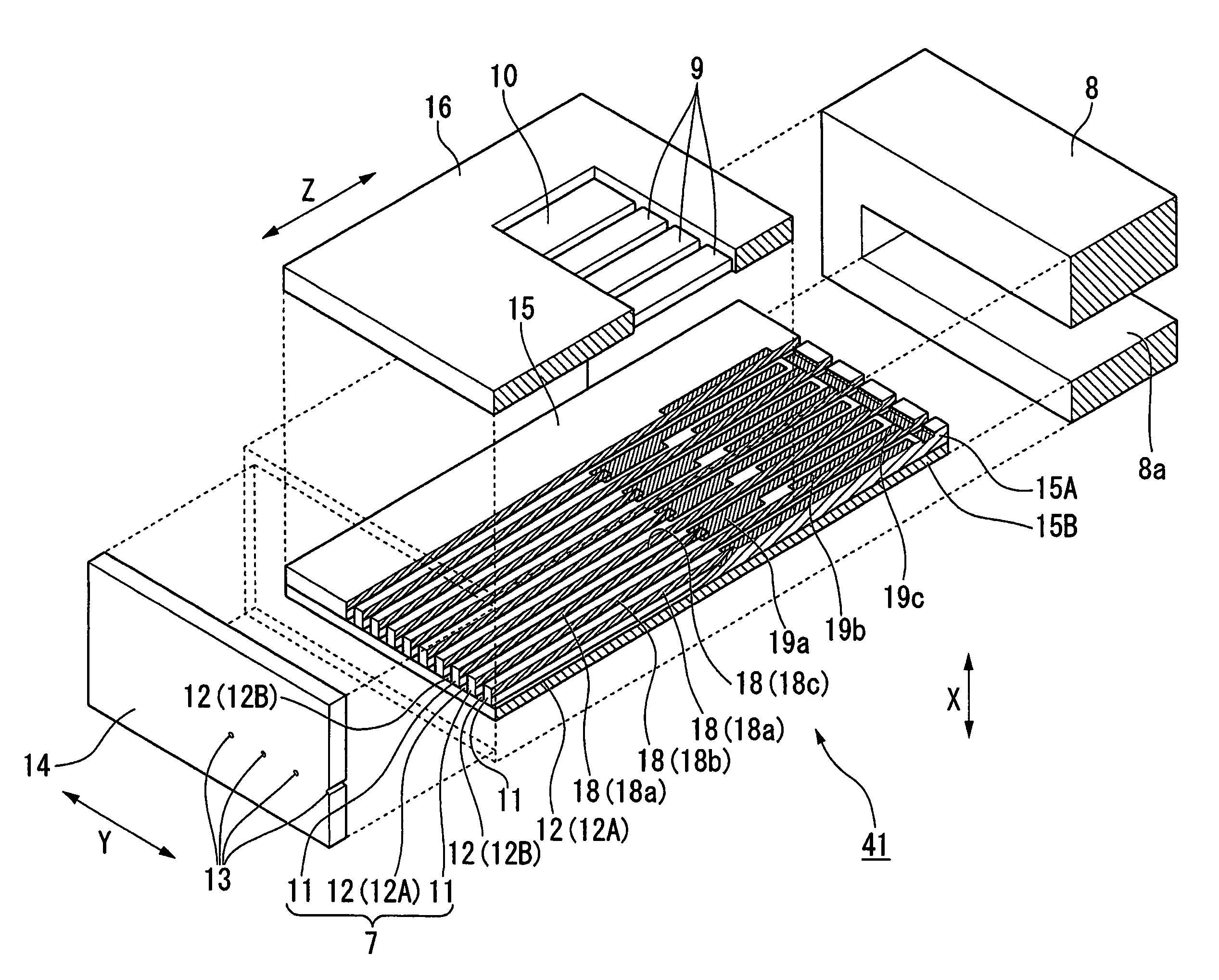
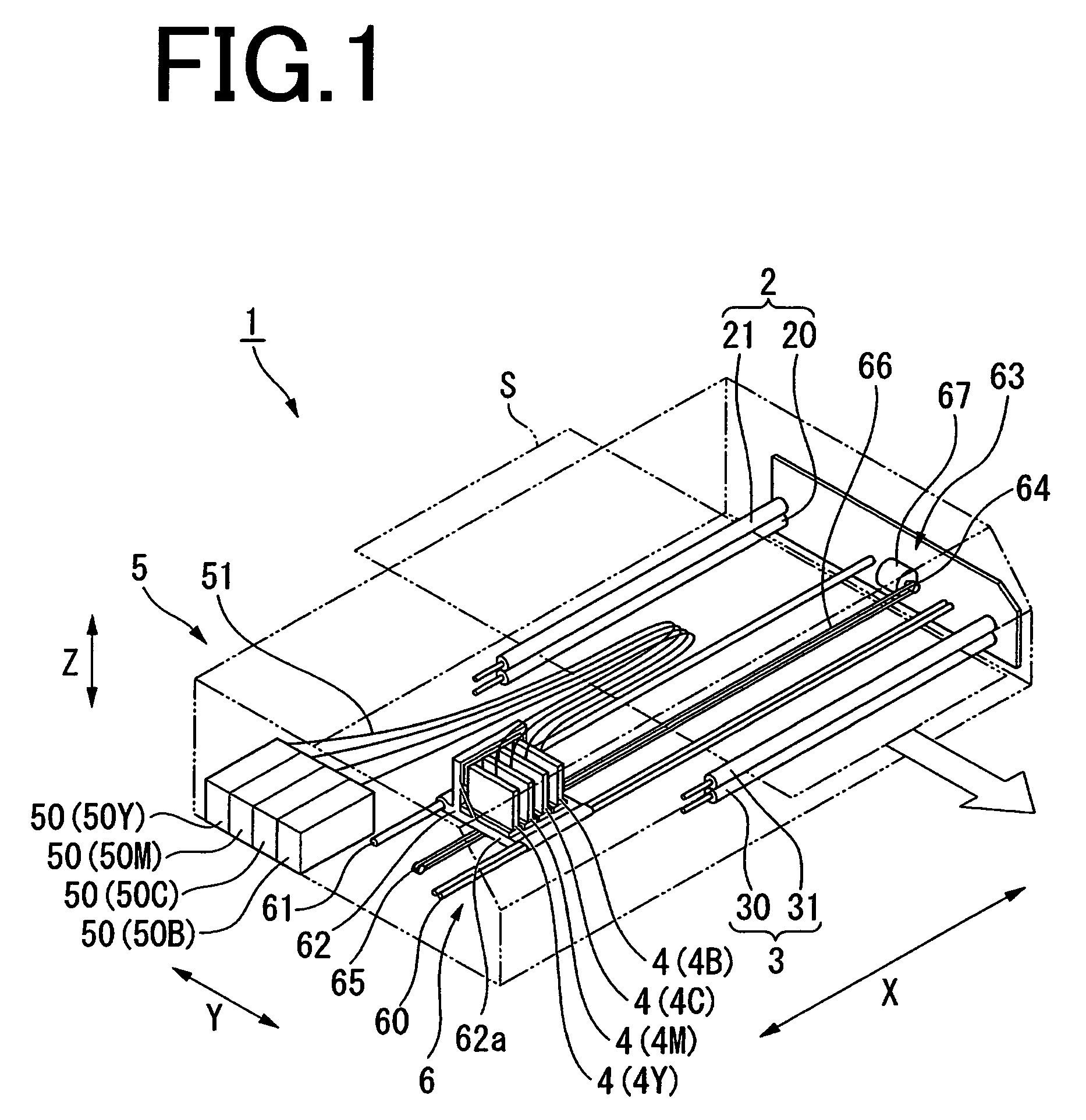
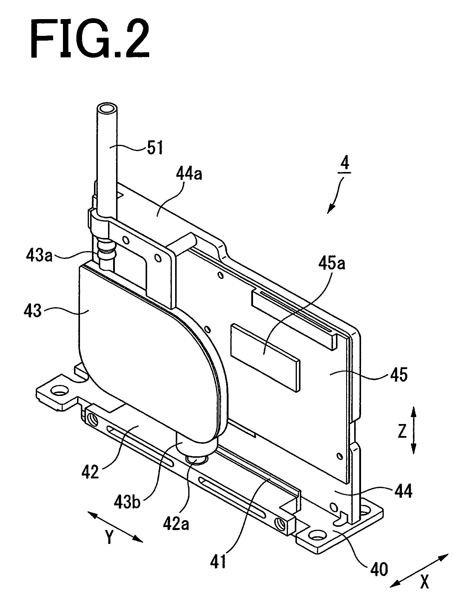
[0038]FIG. 1 is a perspective view illustrating an example of the inkjet recording apparatus according to the present invention. FIG. 2 is a perspective view illustrating the inkjet head including the inkjet head chip according to the present invention. FIG. 3 is a perspective view illustrating an example of the inkjet head chip according to the present invention. FIG. 4 is an exploded perspective view of an inkjet head chip 41 illustrated in FIG. 3. FIG. 5 is a cross-sectional view taken along an arrow A-A of FIG. 3.

[0039]As illustrated in FIG. 1, an inkjet recording apparatus 1 includes a pair of transport means 2 and 3 for transporting a recording medium S such as paper, an inkjet head 4 for discharging ink onto the recording medium S, ink supply means 5 for supplying ink to the inkjet head 4, and scanning means 6 for causing the inkjet head 4 to scan in a direction (hereinafter, referred to as X direction) sub...

second embodiment

[0074]Next, a second embodiment of the present invention is described.

[0075]It should be noted that the second embodiment is similar to the first embodiment described above in the structures other than that of an inkjet head chip 141, and hence the same structures as in the first embodiment are denoted by the same reference numerals and symbols, and their descriptions are omitted.

[0076]FIG. 7 is a cross-sectional view illustrating an example of the inkjet head chip according to the present invention.

[0077]As illustrated in FIG. 7, the inkjet head chip 141 is a so-called shared wall type inkjet head chip in which the discharge channels 12A are successively arranged. The plurality of channels 12 extending in a shorter side direction (Z direction) of the actuator plate 15 are formed at predetermined intervals in the channel parallel direction on one surface (piezoelectric layer 15A side) of the actuator plate 15, and the plurality of channels 12 are each communicating with the nozzle h...

third embodiment

[0083]Next, a third embodiment of the present invention is described.

[0084]It should be noted that the third embodiment is similar to the second embodiment described above in the structures other than that of an actuator plate 115, and hence the same structures as in the first embodiment and the second embodiment are denoted by the same reference numerals and symbols, and their descriptions are omitted.

[0085]FIG. 8 is a partially enlarged perspective view of the actuator plate 115.

[0086]The actuator plate 115 has a structure in which the piezoelectric layer 15A formed of a piezoelectric material and a low-permittivity layer 15C formed of an insulating low-permittivity material are laminated on the low-permittivity substrate layer 15B formed of an insulating low-permittivity material. The piezoelectric layer 15A and the low-permittivity layer 15C are horizontally adjacent to each other. Specifically, the piezoelectric layer 15A is disposed in a distal end portion of the actuator plat...


PUM


Abstract

An inkjet head chip has an actuator plate, discharge channels formed in the actuator plate for discharging ink, and non-discharge channels arranged alternately in parallel with the discharge channels and which are not configured to discharge ink. The actuator plate has a piezoelectric layer and a low-permittivity substrate layer. The piezoelectric layer is formed of a piezoelectric material and the low-permittivity substrate layer is formed of an insulating low-permittivity material having a lower permittivity than that of the piezoelectric material. One end of each discharge channel extends to an end surface of the actuator plate in a state in which the insulating low-permittivity material is exposed on a bottom surface thereof, and another end of each discharge channel does not extend to the end surface of the actuator plate. Each non-discharge channel extends over at least an entire length of the actuator plate in a state in which the insulating low-permittivity material is exposed on a bottom surface thereof. Piezoelectric elements formed of the piezoelectric material are disposed in the discharge and non-discharge channels and driven by a voltage signal for undergoing deformation to vary a volume in the discharge and non-discharge channels to thereby eject ink droplets from the discharge channels.

Description

BACKGROUND OF THE INVENTION[0001]1. Field of the Invention[0002]The present invention relates to a piezoelectric type inkjet head chip for deforming a piezoelectric element through voltage application and boosting a channel internal pressure to discharge an ink droplet through a nozzle hole, a manufacturing method for an inkjet head chip, an inkjet head, and an inkjet recording apparatus.[0003]2. Description of the Related Art[0004]As to the above-mentioned piezoelectric type inkjet head chip, there has been conventionally known a structure including an ink chamber for containing ink, a plurality of piezoelectric elements deformable through voltage application, a plurality of channels partitioned with the piezoelectric elements and formed parallel to each other, and nozzle holes communicating with the channels for discharging an ink droplet toward a recording medium.[0005]Specifically, the inkjet head chip includes an ink chamber plate including the ink chamber formed on one surface...

Claims


Application Information

Patent Timeline
Patent Type & Authority Patents(United States)
IPC IPC(8): B41J2/045
CPCB41J2/14209B41J2/1632B41J2/1609
Inventor KOSEKI, OSAMU
Owner SII PRINTEK
Why Eureka
Try Eureka