System and method for manufacturing double EPI N-type lateral diffusion metal oxide semiconductor transistors

a metal oxide semiconductor and lateral diffusion technology, applied in the field of semiconductor devices, can solve the problems of inability to simultaneously achieve a wide base width and a high doping concentration, unsatisfactory modes of operation, and latching problems, and achieve the effect of reducing and minimizing the effect of parasitic bipolar transistors

Active Publication Date: 2011-06-14
NAT SEMICON CORP
View PDF10 Cites 17 Cited by
  • Summary
  • Abstract
  • Description
  • Claims
  • Application Information

AI Technical Summary

Benefits of technology

[0013]To address the above-discussed deficiencies of the prior art, it is a primary object of the present invention to provide a manufacturing method that reduces and minimizes the effect of parasitic bipolar transistors within lateral diffusion metal oxide semiconductor (LDMOS) transistors.

Problems solved by technology

Undesirable modes of operation may occur in a DMOS transistor.
These parasitic modes of operation may take the form of an undesirable parasitic bipolar transistor that is formed within the structure of the DMOS transistor.
The presence of this parasitic PNP bipolar transistor 110 can cause latch up problems in the operation of the N-type lateral DMOS device 100.
The presence of this parasitic NPN bipolar transistor 120 can also cause malfunctions in the operation of the N-type lateral DMOS device 100.
This means that it is not possible to simultaneously achieve a wide base width and a high doping concentration.
This prior art approach has a significant limitation in that it is not possible to achieve both a wide base width and a high doping concentration at the same time.
This prior art approach has a significant limitation in that it is not possible to completely stop the current that is due to the presence of the parasitic NPN bipolar transistor 120.

Method used


Image

  • System and method for manufacturing double EPI N-type lateral diffusion metal oxide semiconductor transistors
  • System and method for manufacturing double EPI N-type lateral diffusion metal oxide semiconductor transistors
  • System and method for manufacturing double EPI N-type lateral diffusion metal oxide semiconductor transistors

Examples


Embodiment Construction

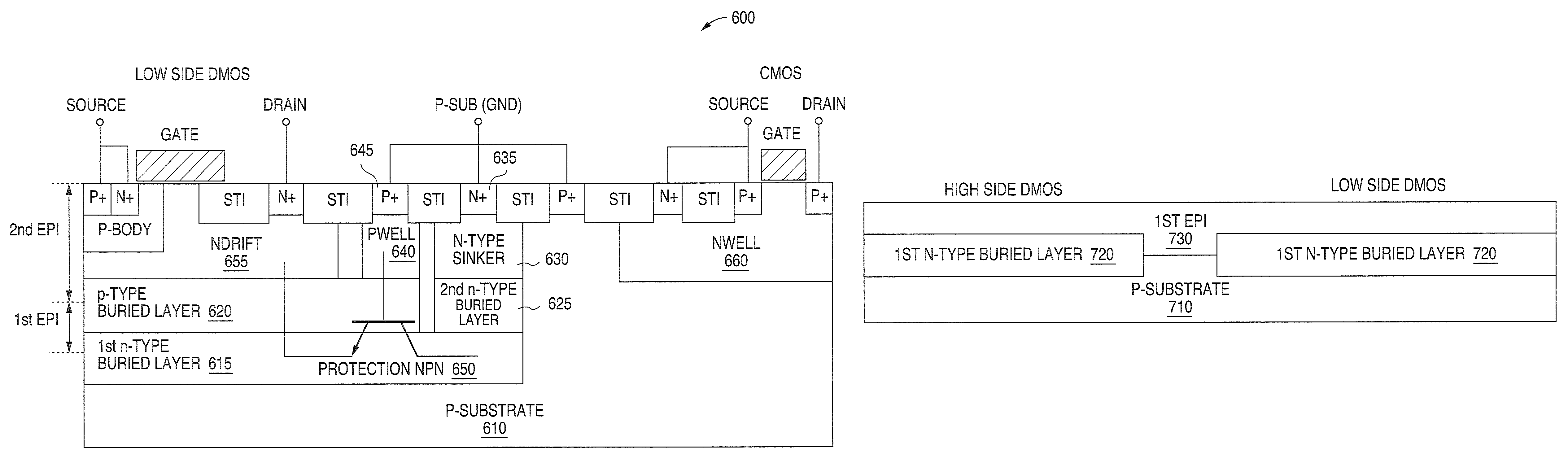
[0028]FIGS. 5 through 13 and the various embodiments used to describe the principles of the present invention in this patent document are by way of illustration only and should not be construed in any way to limit the scope of the invention. Those skilled in the art will understand that the principles of the present invention may be implemented in any type of suitably arranged lateral diffusion metal oxide semiconductor (LDMOS) transistor device. To simplify the drawings the reference numerals from previous drawings will sometimes not be repeated for structures that have already been identified.

[0029]The method of the present invention for manufacturing an N-type lateral diffusion metal oxide semiconductor (LDMOS) transistor device creates two N-type buried layers and creates two epitaxial layers. The method of manufacture will be described in more detail later in this patent document.

[0030]FIG. 5 is a schematic cross sectional view showing an advantageous embodiment of an N-type la...


PUM


Abstract

A system and a method are disclosed for manufacturing double epitaxial layer N-type lateral diffusion metal oxide semiconductor transistors. In one embodiment two N-type buried layers are used to minimize the operation of a parasitic PNP bipolar transistor. The use of two N-type buried layers increases the base width of the parasitic PNP bipolar transistor without significantly decreasing the peak doping profiles in the two N-type buried layers. In one embodiment two N-type buried layers and one P-type buried layer are used to form a protection NPN bipolar transistor that minimizes the operation of parasitic NPN bipolar transistor. The N-type lateral diffusion metal oxide semiconductor transistors of the invention are useful in inductive full load or half bridge converter circuits that drive very high current.

Description

TECHNICAL FIELD OF THE INVENTION[0001]The present invention is generally directed to methods for manufacturing semiconductor devices and, in particular, to a system and method for manufacturing double epitaxial layer N-type lateral diffusion metal oxide semiconductor transistors.BACKGROUND OF THE INVENTION[0002]In the semiconductor manufacturing industry diffusion metal oxide semiconductor (DMOS) transistors are commonly used in power integrated circuits. A DMOS transistor comprises a source region and a body region. During the manufacture of a DMOS transistor the source region and the body region are simultaneously diffused so that the channel length of the DMOS transistor is defined by the difference between the two diffusion lengths. The double diffusion feature of the DMOS transistor permits a short channel region to be formed that can control large drain currents by the gate voltage of the DMOS transistor. In a DMOS transistor a drift region is formed between the short channel ...

Claims


Application Information

Patent Timeline
Patent Type & Authority Patents(United States)
IPC IPC(8): H01L21/336
CPCH01L21/823418H01L21/823456H01L21/823493H01L27/0921H01L27/0928H01L29/7817H01L29/0878H01L29/1083H01L29/1087H01L29/66681H01L29/7816H01L29/0653
Inventor KWON, TAEHUN
Owner NAT SEMICON CORP
Why Eureka
Try Eureka