Cooling device for electronic component and power converter equipped with the same

a technology of cooling device and electronic component, which is applied in the direction of power cables, cables, lighting and heating apparatus, etc., can solve the problems of difficult downsizing of power conversion device, requiring a different cooling efficiency, and not uniform heat value of modules, so as to prevent thermal interference and facilitate the regulation of the cooling efficiency of electronic components.

Inactive Publication Date: 2011-06-21
DENSO CORP
View PDF29 Cites 38 Cited by
  • Summary
  • Abstract
  • Description
  • Claims
  • Application Information

AI Technical Summary

Benefits of technology

[0012]With the foregoing difficulties in view, an object of the present invention is to provide a cooling device, which is capable of preventing thermal interference between the adjacent electronic components and also is easy to regulate the cooling efficiency of the electronic components.

Problems solved by technology

However, due to the use of the presser plates and the spring member, the spacing between a stacked or laminated array of semiconductor modules is relatively large, making it difficult to downsize the power conversion device.
It may occur, however, that the plural semiconductor modules are not uniform in heat value and hence require a different cooling efficiency provided for each of the semiconductor module.
In this instance, the foregoing arrangement is not convenient because the pressure acting between the semiconductor modules and the cooling tubes is uniform throughout the assembly.
If the pressure is set to be suitable for a semiconductor module having a maximum heat value, an excessively large pressure will be applied to the entire laminated assembly.
This arrangement, however, lacks versatility because of the design requirements in which a thermal balance must be provided for a plurality of different circuit control patterns in view of the thermal interference between the adjacent semiconductor modules and the difference in flow distribution of the cooling medium.
This arrangement is, however, difficult to realize because the entire coolant circulation path requires a high pressure-proof design.
Furthermore, since the pressure applied from the cooling tube to the respective electronic components is uniform throughout the electronic component and cooling tube assembly, the same problem as the one discussed above with respect to JP 2005-191082A will occur.

Method used


Image

  • Cooling device for electronic component and power converter equipped with the same
  • Cooling device for electronic component and power converter equipped with the same
  • Cooling device for electronic component and power converter equipped with the same

Examples


first embodiment

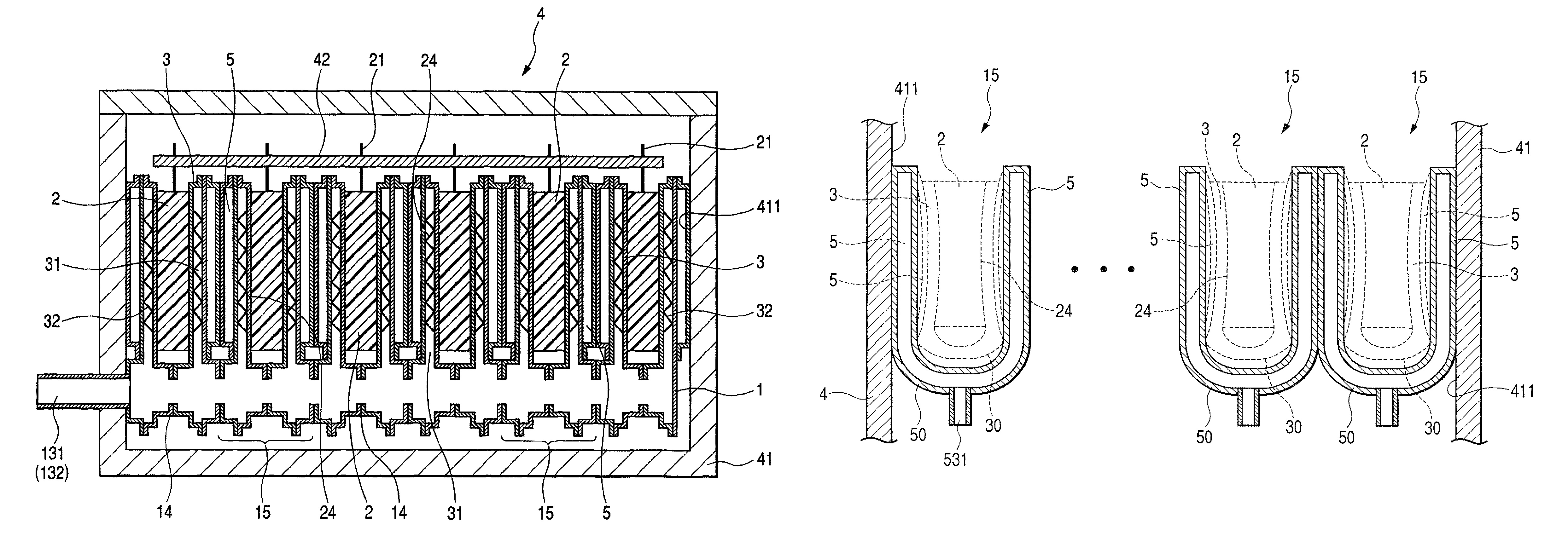
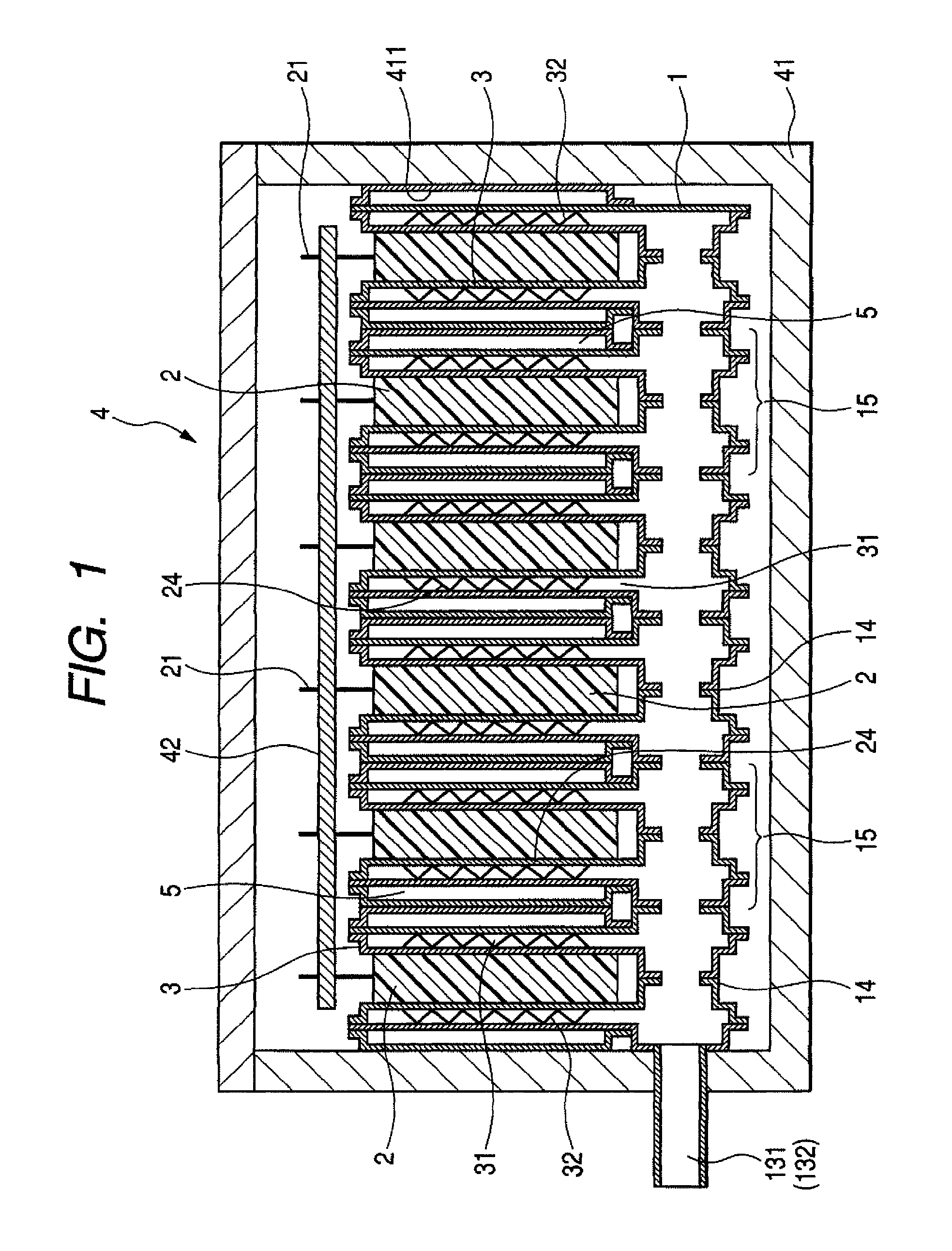
[0071]Referring now to the drawings, wherein like reference characters designate like or corresponding parts throughout the several views, FIG. 1 shows a cooling device for an electronic component and an electric power converting device or converter equipped with the cooling device according to a first embodiment of the present invention.

[0072]In this embodiment, the cooling device 1 takes the form of a cooling device so configured as to cool semiconductor modules as electronic components. The cooling device 1 comprises a cooling tube 3 disposed in contact with each of the semiconductor modules 2 and having an internal coolant flow channel 31 for the passage therethrough of a cooling medium or coolant, and a high-pressure tube 5 disposed adjacent to a surface of the cooling tube 3 that faces away from the associated semiconductor module 2. The high-pressure tube 5 has a hollow interior that can be filled with a high-pressure fluid.

[0073]The cooling tube 3 is disposed in contact with...

second embodiment

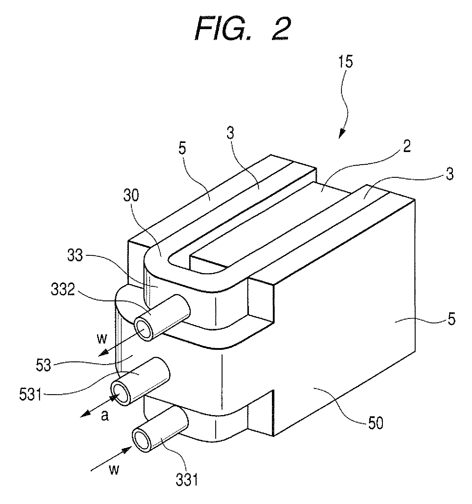
[0091]A second embodiment of the invention will be described below with reference to FIGS. 2 to 5. As shown in FIGS. 2 and 3, a pair of cooling tubes 3 and 3 is in contact with both surfaces (heat radiating surfaces) of a semiconductor module 2. The cooling tubes 3 are formed by part of a tube 30 of U-shaped configuration having a pair of straight stems and a bent portion 33 interconnecting the straight stems at one end thereof. More particularly, the cooling tubes 3, 3 are formed by the straight stems of the U-shaped tube 30. Similarly, as shown in FIGS. 2 and 4, a pair of high-pressure tubes 5 and 5 is in contact with the pair of cooling tubes 3, 3, respectively. The high-pressure tubes 5, 5 are formed by part of a tube 50 of U-shaped configuration having a pair of straight stems and a bent portion 53 interconnecting the straight stems at one end thereof. More particularly, the high-pressure tubes 5, 5 are formed by the straight stems of the U-shaped tube 50.

[0092]As shown in FIGS...

third embodiment

[0099]FIG. 6 shows a semiconductor cooling unit 15 according to a third embodiment of the present invention. The semiconductor cooling unit 15 of this embodiment is substantially the same in construction as the semiconductor cooling unit of the second embodiment shown in FIG. 2 with the exception that the U-shaped tube 30 forming a pair of cooling tubes 3 and 3 is received or nested in the U-shaped tube 30 forming a pair of high-pressure tubes 5 and 5 with the respective bent portions 33, 55 disposed on opposite sides of the semiconductor module 2.

[0100]With this arrangement, the bent portion 53 of the U-shaped tube 50 does not interfere with the coolant inlet and outlet portions 331, 332 and hence this bent portion 53 is not narrowed in width but has the same width as the bent portion 33 of the U-shaped tube 30.

[0101]Other parts of the third embodiment are the same as those described above with respect to the second embodiment and further description thereof can be omitted. Due to ...


PUM


Abstract

A cooling device for cooling an electronic component (semiconductor module) includes a cooling tube adapted to be disposed in contact with the electronic component and having an internal coolant flow channel for the passage therethrough of a cooling medium, and a high-pressure tube disposed adjacent to a surface of the cooling tube that faces away from the electronic component, the high-pressure tube having a hollow interior that can be filled with a high-pressure fluid having a pressure higher than that of the cooling medium. An electric power conversion device comprised of a plurality of semiconductor modules and the cooling device as means for cooling the semiconductor modules is also disclosed.

Description

CROSS REFERENCE TO RELATED APPLICATION[0001]The present application is based on and claims priority from Japanese Patent Applications No. 2007-82587, filed Mar. 27, 2007, and No. 2007-262805, filed Oct. 8, 2007, the contents of which are incorporated herein by reference.BACKGROUND OF THE INVENTION[0002]1. Field of the Invention[0003]The present invention relates to a cooling device for cooling an electronic component such as a semiconductor module, and a power conversion device or converter equipped with the cooling device.[0004]2. Description of the Related Art[0005]Electric power conversion devices, such as inverters, converters and so on, that are equipped with a plurality of semiconductor modules with semiconductors incorporated therein and a cooling device for cooling the semiconductor modules are known heretofore.[0006]One example of such known power conversion devices is disclosed in Japanese Patent Laid-open Publication (JP-A) No. 2001-320005 (corresponding to U.S. Pat. No. ...

Claims


Application Information

Patent Timeline
Patent Type & Authority Patents(United States)
IPC IPC(8): H05K7/20
CPCH01L23/473H01L25/117H01L2924/0002H01L2924/00
Inventor YAMAMOTO, TAKESHIINOUE, SEIJIFUKATSU, YOSHIAKI
Owner DENSO CORP
Why Eureka
Try Eureka