Laser compression bonding device and method for semiconductor chip

a laser compression bonding and semiconductor chip technology, applied in the direction of manufacturing tools, metal working devices, television systems, etc., can solve problems such as disadvantages such as warping, and achieve the effects of improving bonding equality, uniform pitch between bumps, and improving banding quality

Active Publication Date: 2022-01-20
ML EQUIP KOREA CO LTD
View PDF0 Cites 2 Cited by
  • Summary
  • Abstract
  • Description
  • Claims
  • Application Information

AI Technical Summary

Benefits of technology

[0019]According to another aspect of the present invention, there is provided a laser compression bonding method of bonding a semiconductor chip to a substrate using the laser compression bonding device described above, the method including: moving down a bonding tool at a high speed from an initial position to a predetermined height for low-speed start-up; moving down the bonding tool at a low speed from the height for low-speed start-up to a height for lowest-speed start-up; moving down the bonding tool at a lowest speed from the height for lowest-speed start-up to a height for contact with a semiconductor chip D; determining that the bonding tool is brought into contact with the semiconductor chip D, when the bonding tool is moved down at the lowest speed to the height for contact with the semiconductor chip D and then a load cell detects that a pressure against the semiconductor chip D reaches 5 N/cm2, and enabling a laser beam generator to operate to emit a laser beam, thereby performing bonding, when a target input value necessary for bonding at a pressure of 5 N/cm2 is input; and moving up the bonding tool to a height for finishing a bonding operation, thereby finishing the bonding ope...

Problems solved by technology

This warping is a disadvan...

Method used


Image

  • Laser compression bonding device and method for semiconductor chip
  • Laser compression bonding device and method for semiconductor chip
  • Laser compression bonding device and method for semiconductor chip

Examples


Embodiment Construction

[0032]A preferable embodiment of the present invention will be described in detail below with reference to the accompanying drawings.

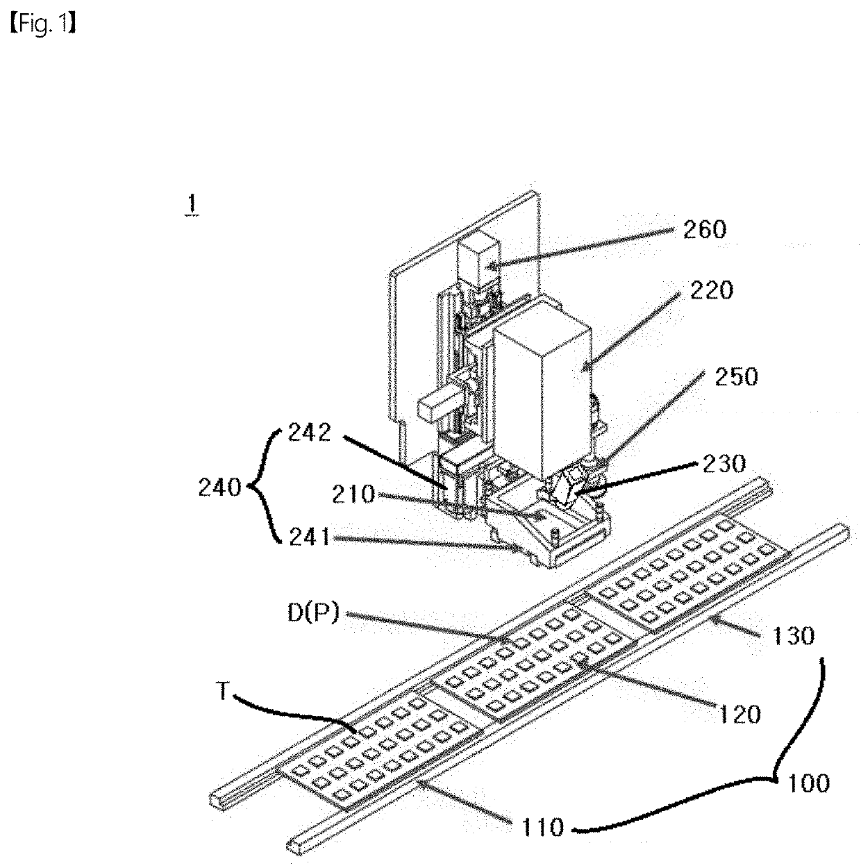
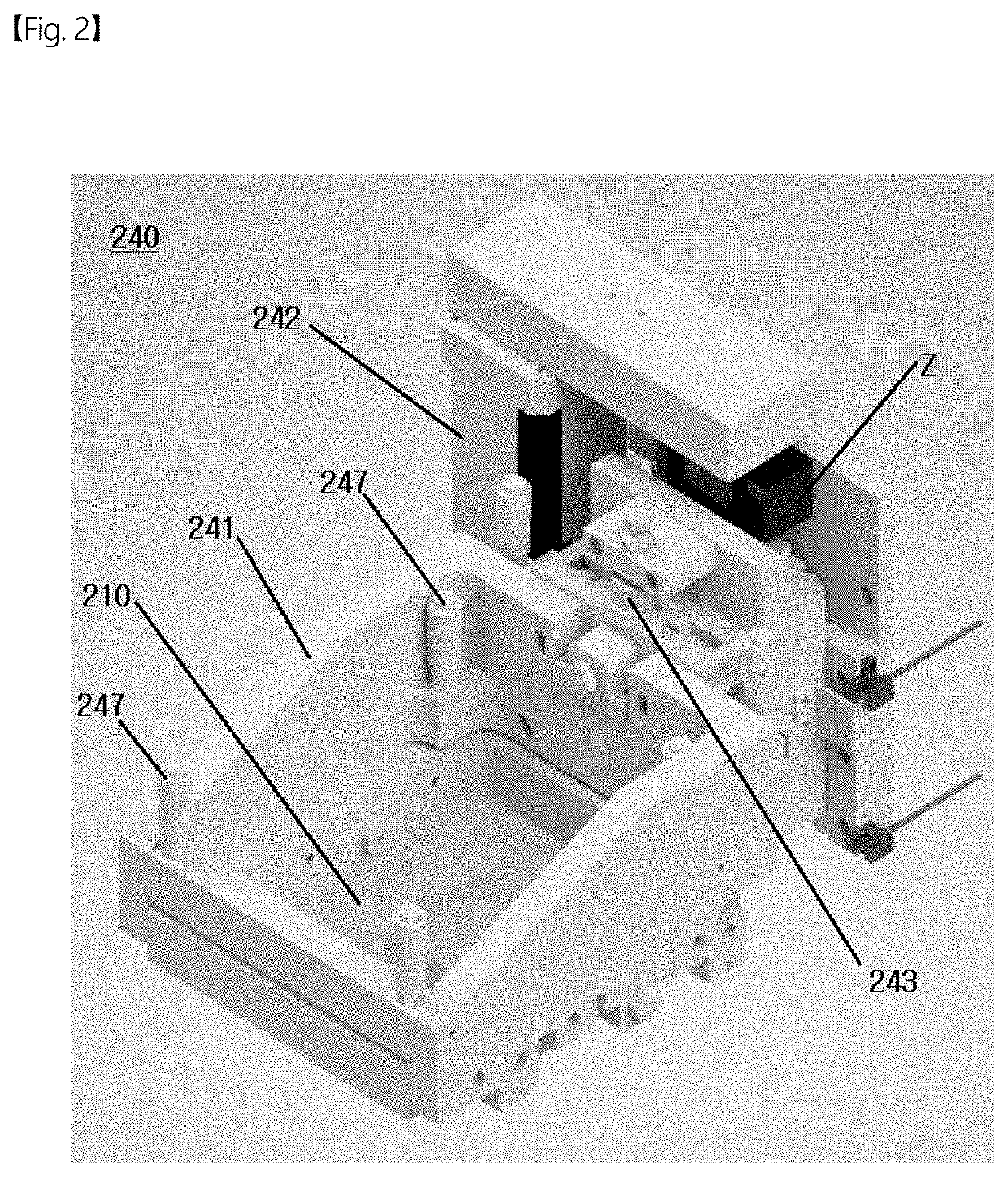
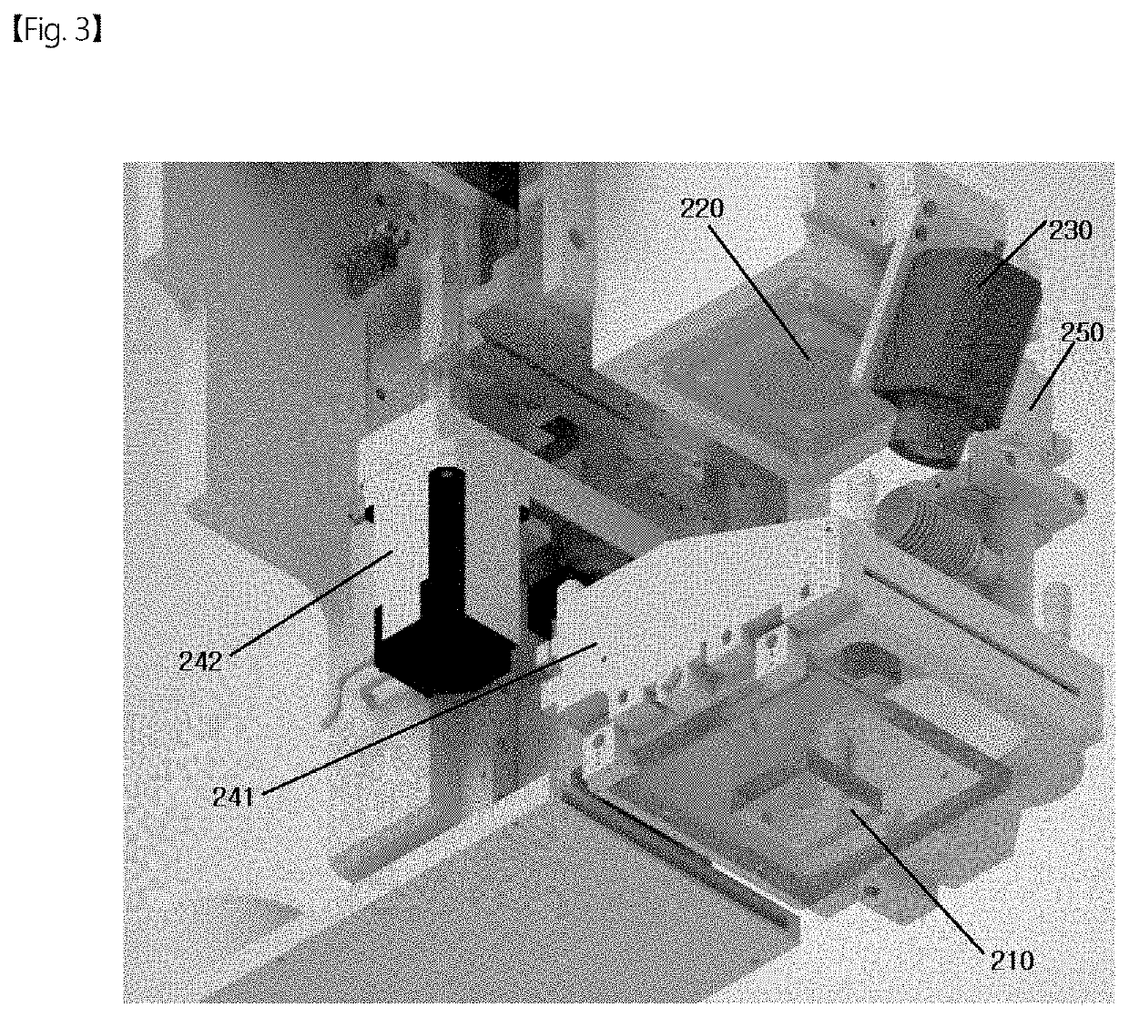
[0033]FIG. 1 illustrates a schematic configuration of a laser compression bonding device according to the present invention. FIG. 2 illustrates a lower portion of the bonding head in FIG. 1 in an enlarged manner. FIG. 3 illustrates a bottom of the lower portion of the bonding head in FIG. 1 in an enlarged manner.

[0034]As illustrated, a laser compression bonding device 1 according to the present invention includes a conveyor unit 100 and a bonding head 200. The conveyor unit 100 is configured to transport a semiconductor chip (die) D and a substrates P from a pre-bonding zone 110 through a main bonding zone 120 to an unloading zone 130. The semiconductor chip D and the substrate P are received in the pre-bonding zone 110.

[0035]The bonding head 200 includes a bonding tool 210, a laser beam generator 220, a thermal imaging camera 230, and a compression un...


PUM

PropertyMeasurementUnit
Fractionaaaaaaaaaa
Pressureaaaaaaaaaa
Temperatureaaaaaaaaaa

Abstract

A laser compression bonding device and method for a semiconductor chip are proposed. The device includes a conveyor unit that transports a semiconductor chip and a substrate, and a bonding head that includes a bonding tool for applying a pressure to the chip and substrate, a laser beam generator for emitting a laser beam, a thermal imaging camera for measuring temperatures of the surfaces of semiconductor chip and substrate, and a compression unit for controlling a pressure applied by the bonding tool and a position thereof, wherein the compression unit includes a mount on which the bonding tool is detachably mounted, and a servo motor and a load cell that apply a pressure to the mount or control a position thereof. The servo motor is controlled with two values for pressure application and positioning.

Description

CROSS REFERENCE TO RELATED APPLICATION[0001]The present application claims priority to Korean Patent Application No. 10-2020-0087077, filed Jul. 14, 2020, the entire contents of which is incorporated herein for all purposes by this reference.BACKGROUND OF THE INVENTIONField of the Invention[0002]The present invention relates to a laser compression bonding device for and a laser compression bonding method of bonding a semiconductor chip of size 100 micrometers or less to a substrate, and more particularly, to a laser compression bonding device for and a laser compression bonding method of bonding a semiconductor chip to a substrate while warping of the semiconductor chip and the substrate that occurs when performing laser bonding is suppressed effectively through control of a pressure applied by a bonding tool and control of a position thereof.Description of the Related Art[0003]Generally, a flip chip bonding process is performed by causing a bump structure called a lead-free solder ...

Claims


Application Information

Patent Timeline
IPC IPC(8): H01L23/00B23K26/20
CPCH01L24/75B23K2101/40B23K26/20H01L24/81B23K26/21B23K26/702B23K26/032B23K26/034H01L2224/75001H01L2224/75263H01L2224/753H01L2224/75313H01L2224/75821H01L2224/75841H01L2224/759H01L2224/7592H01L2224/81203H01L2224/81224H01L2224/81801H01L2924/3511H01L2224/81908H01L2224/75901H01L2224/7565H01L2224/75262H01L2224/75251H01L2224/131H01L24/16H01L24/13H01L2224/16227B23K26/0838H01L2924/014H01L2924/00014H01L23/562H04N5/33
Inventor PARK, JAE SHINOH, KUANG ENG
Owner ML EQUIP KOREA CO LTD
Why Eureka
Try Eureka