Method for manufacturing electro-optical device, electro-optical device, and electronic equipment

a manufacturing method and technology for optical devices, applied in the direction of radiation controlled devices, identification means, instruments, etc., can solve the problems of affecting the performance of optical devices, degrading the characteristics of optical devices, and affecting the quality of optical devices

Inactive Publication Date: 2002-03-19
138 EAST LCD ADVANCEMENTS LTD
View PDF4 Cites 46 Cited by
  • Summary
  • Abstract
  • Description
  • Claims
  • Application Information

AI Technical Summary

Benefits of technology

In accordance with the manufacturing method of the present invention, the light shielding layer formed on one side of the light transmissive substrate is present not in either the formation area of the transistor element or in the peripheral area of the transistor element, and variations of protrusions of the substrate due to the light shielding layer are reduced. A uniformity in the polishing rate on the substrate is substantially improved when the insulating layer on the light shielding layer is planarized through the polishing process. Through the planarizing process of the insulating layer, the surface of the light transmissive substrate is thus planarized to be flat without introducing waviness therein. No void occurs in the interface between the insulating layer and the monocrystalline silicon layer, the bond between the insulating layer and the monocrystalline silicon layer increases, and the transistor element is thus free from variations in performance characteristics and failures.
In accordance with the present invention, the surface of the insulating layer is thus planarized to be flat. No void occurs in the interface between the insulating layer and the monocrystalline silicon layer. An electro-optical device features a strong bond between the insulating layer and the monocrystalline silicon layer, with the transistor element free from variations in the performance characteristics and failures.
Since the protruded state of the surface of the insulating layer in the area where no transistor elements are formed is similar to the protruded state of the transistor formation area before planarization in this arrangement of the present invention, uniformity in the polishing rate is improved, and surface waviness is reduced prior to the planarizing process. No void occurs in the interface between the insulating layer and the monocrystalline silicon layer. An electro-optical device features a strong bond between the insulating layer and the monocrystalline layer with the transistor element free from variations in the characteristics and failures.
In the electro-optical device of the present invention, the light transmissive substrate is fabricated of quartz, and the light shielding layer is fabricated of a refractory metal or a refractory metal-silicide. In the transistor formation process on the light shielding layer, a heat treatment above 1000.degree. C. can be performed to improve the device performance characteristics.
In accordance with the manufacturing method of the present invention, the pattern of the light shielding layer is present both in the formation area of the transistor element and in the peripheral area of the transistor element, and variations in the distribution of protrusions of the substrate due to the light shielding layer are small. A uniformity in the polishing rate on the substrate is substantially improved when the insulating layer on the light shielding layer is planarized through the polishing process. Since the peripheral area is easy to polish during the planarizing process, arranging the light shielding layer in the peripheral area reduces the variations in the distribution of protrusions in the substrate. No void occurs in the interface between the insulating layer and the monocrystalline silicon layer, the bond between the insulating layer and the monocrystalline silicon layer is increased, and the transistor element is thus free from variations in the performance characteristics and failures. Additionally, by arranging the light shielding layer in the area facing the drive circuit, no light is permitted to enter the drive circuit, and the transistor formed in the drive circuit is free from erratic operations.
Since the light shielding layer arranged in the area facing the transistor and the light shielding layer arranged in the area facing the drive circuit have generally identical shapes in accordance with the manufacturing method of the present invention, the spacings between the light shielding layers become substantially uniform, and the degree of waviness is further reduced through the planarizing process of the insulating layer thereon.

Problems solved by technology

Although the returning light is a mere fraction of the light quantity of light incident on the surface of the substrate, it is strong enough to cause a leakage photocurrent in an apparatus, such as a projector, which handles a high-power light source.
The returning light from the back surface adversely affects the switching characteristics of the element, thereby degrading the device characteristics.
As a result, the insulating layer suffers from waviness in the surface thereof subsequent to the polishing process.
If the insulating layer suffers from the waviness on the surface thereof, the following problems arise.
First, a void is caused in the interface with the insulating layer and the monocrystalline silicon layer, and the MOSFET formed in the void suffers from poor performance characteristics or suffers from a complete failure.
Second, the bond between the insulating layer and the monocrystalline silicon layer is weakened.
A weakened bond in the MOSFET forming process subsequent to the formation of the monocrystalline silicon layer, causes a failure such as a peel of the monocrystalline silicon layer thereby decreasing the production yield of the device.
Since no light shielding layer is arranged in the area facing the drive circuit and the external-circuit interconnect terminal, the electrical effect caused by the light shielding layer is limited.

Method used


Image

  • Method for manufacturing electro-optical device, electro-optical device, and electronic equipment
  • Method for manufacturing electro-optical device, electro-optical device, and electronic equipment
  • Method for manufacturing electro-optical device, electro-optical device, and electronic equipment

Examples


Embodiment Construction

The embodiments of the present invention are now discussed, referring to the drawings.

(Basic Construction of the Electro-optical Device)

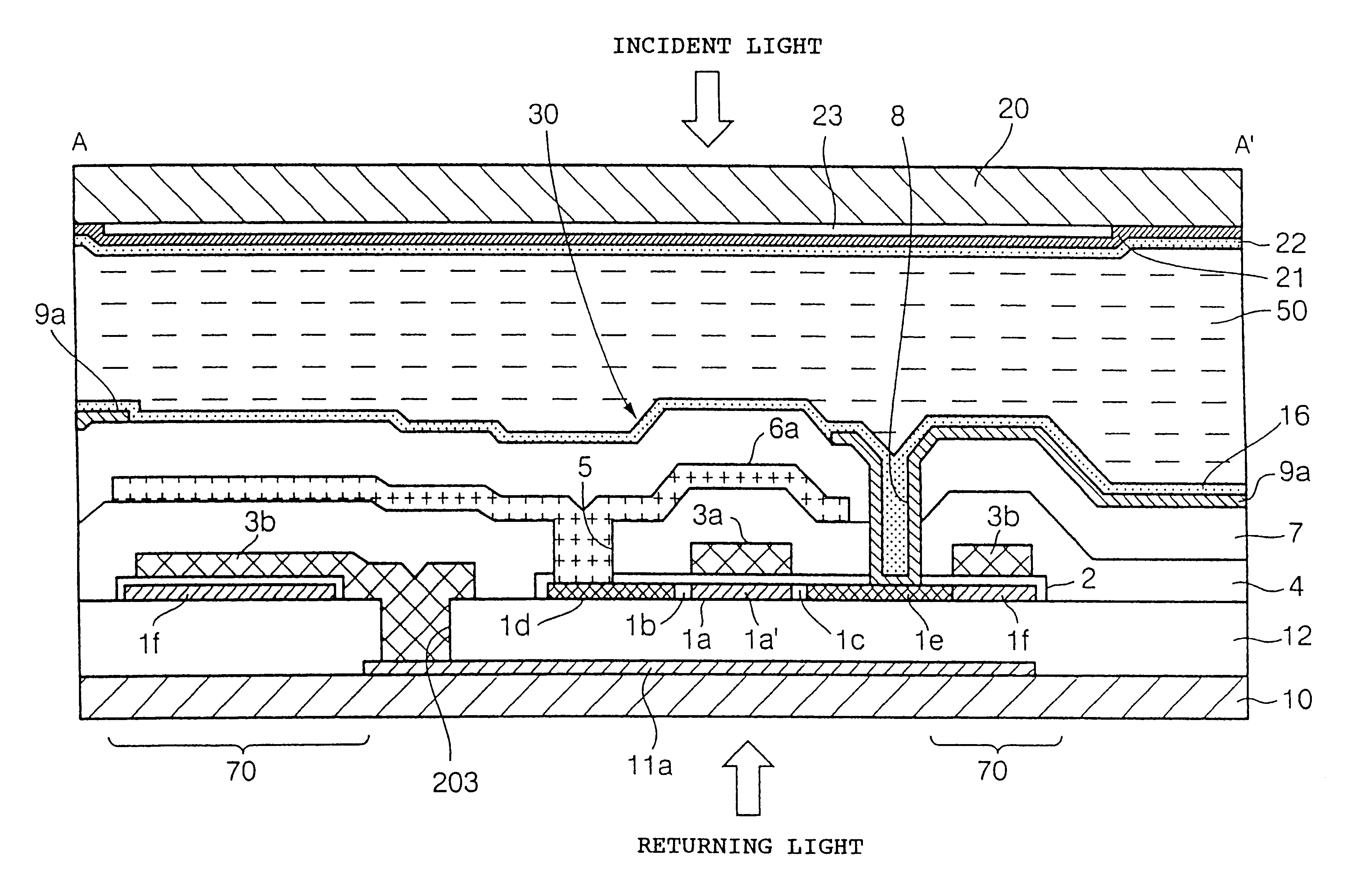
FIG. 1 is a cross-sectional view showing the basic construction of the electro-optical device of a first embodiment of the present invention.

Referring to FIG. 1, an electro-optical device 201 includes a light shielding layer 204 formed on a light transmissive substrate (transparent substrate) 202. An insulating layer 205 and a monocrystalline silicon layer 206 are successively formed on the light transmissive substrate 202. A transistor element formation region (not shown) is formed in the monocrystalline silicon layer 206 in a position corresponding to the light shielding layer 204.

(Manufacturing Process)

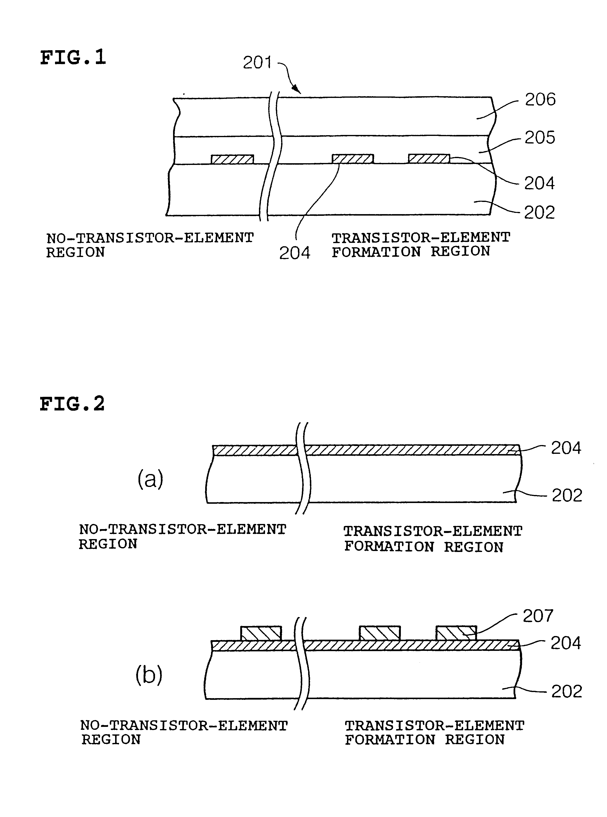
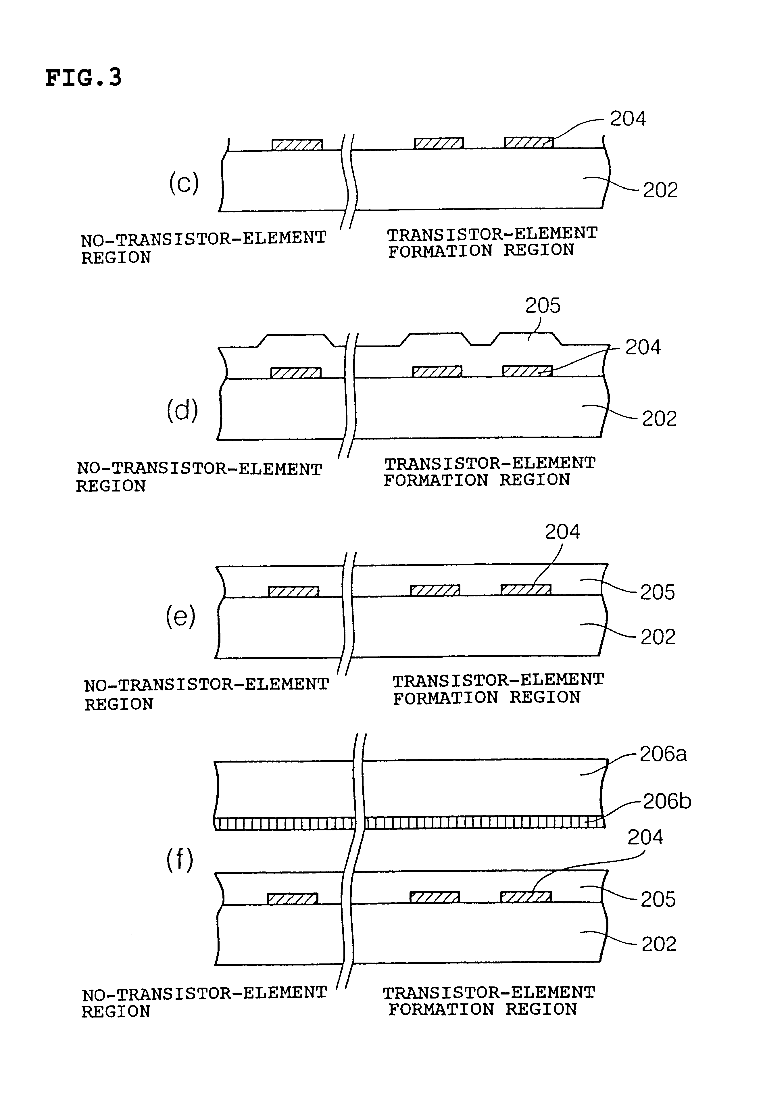
The manufacturing process of the above electro-optical device is now discussed, referring to FIG. 2 step (2) through FIG. 4 step (g)

Referring to FIG. 2 step (2), the light shielding layer 204 is formed on the entire top surface of the transparent l...


PUM

PropertyMeasurementUnit
thicknessaaaaaaaaaa
thicknessaaaaaaaaaa
thicknessaaaaaaaaaa

Abstract

A electro-optical device and manufacturing method are provided for an electro-optical device that has the step of forming a light shielding layer on one side of a light transmissive substrate, patterning the light shielding layer, forming an insulating layer on the patterned light shielding layer, planarizing the insulating layer, bonding a model crystalline silicon layer on the surface of the planarized insulating layer, and forming a transistor element from the monocrystalline silicon layer, wherein the patterned light shielding layer is arranged in an area facing the transistor element and in a peripheral area surrounding the transistor element.

Description

1. Field of the InventionThe present invention relates to a method for manufacturing an electro-optical device having a light transmissive substrate and a monocrystalline layer bonded to the substrate, the electro-optical device and electronic equipment. In particular, the present invention relates to a method for manufacturing an electro-optical device having a light shielding layer formed on a light transmissive substrate, the electro-optical device and electronic equipment.2. Description of the Related ArtThe SOI technology in which a seminconductor device is formed on a silicon thin film on top of an insulating substrate is appropriate for use in an electro-optical device such as a liquid-crystal display device, because the SOI technology offers high-speed, low-power consumption features and the high degree of integration in devices.When the SOI technology is applied to the electro-optical device, a monocrystalline silicon substrate is bonded to a light transmissive substrate, a...

Claims


Application Information

Patent Timeline
Patent Type & Authority Patents(United States)
IPC IPC(8): G02F1/13G02F1/1362H01L27/146G02F1/136G02F1/1368G09F9/00G09F9/30H01L21/336H01L29/786
CPCG02F1/136209H01L27/14645H01L27/14609H01L27/14623G02F1/136213G02F2001/13613G02F1/13613
Inventor HIRABAYASHI, YUKIYA
Owner 138 EAST LCD ADVANCEMENTS LTD
Why Eureka
Try Eureka