Semiconductor device

a semiconductor and device technology, applied in semiconductor devices, semiconductor/solid-state device details, electrical devices, etc., can solve the problems of increasing insufficient resolution, and increasing so as to reduce the size and cost of semiconductor devices, and reduce the variation of lithography and complicated designs.

Inactive Publication Date: 2010-02-25
RENESAS ELECTRONICS CORP
View PDF2 Cites 44 Cited by
  • Summary
  • Abstract
  • Description
  • Claims
  • Application Information

AI Technical Summary

Benefits of technology

[0010]The present invention has been made in view of the above disadvantage, and one object thereof is to provide a semiconductor device that can reduce / eliminate variation in lithography and complicated designs while reducing the semiconductor device's size and cost.
[0011]Furthermore, another object of the present invention is to provide a semiconductor device that can ensure resolution and stability in lithography for a design with cells highly integrated.
[0017]The present invention in one embodiment provides a semiconductor device in which a first virtual line of a plurality of first virtual lines that is the closest to a boundary and a second virtual line of a plurality of second virtual lines that is the closest to the boundary have therebetween a spacing larger than a single pitch. If it is necessary that the first virtual line that is the closest to the boundary and the second virtual line that is the closest to the boundary be sufficiently spaced from each other, the single pitch can be suppressed. The semiconductor device's size and cost can thus be reduced.
[0018]The present invention in another embodiment provides a semiconductor device in which a spacing between a first virtual line of a plurality of first virtual lines that is the closest to a first peripheral edge and the first peripheral edge and a spacing between a second virtual line of a plurality of second virtual lines that is the closest to a second peripheral edge and the second peripheral edge are each larger than a single pitch. If it is necessary that the first virtual line that is the closest to the first peripheral edge and the first peripheral edge be sufficiently spaced from each other and so be the second virtual line that is the closest to the second peripheral edge and the second peripheral edge, the single pitch can be suppressed. The semiconductor device's size and cost can thus be reduced.
[0019]The present invention in still another embodiment provides a semiconductor device having a plurality of cells each having a width of an integral multiple of a first pitch in a first direction. This allows a region filled with a plurality of cells to have gate electrodes arranged with uniform pitches. This allows a design with cells highly integrated to also ensure resolution and stability in lithography.

Problems solved by technology

This results in making it difficult to ensure resolution in lithography for the 45 nm or 32 nm or later generation in particular.
This problem is remarkable in particular for general SOC products, which have a chip having a large area occupied by standard cells.
In other words, the chip has a major area occupied by standard cells having an increased area, and as a consequence, the chip is increased in size, resulting in a semiconductor device increased in size and cost.
Furthermore, simply making a cell that has conventionally been used fine in a design for the purpose of highly integrating a semiconductor device has resulted in insufficient resolution and increased variation in lithography.
There has not been a sufficient proposal for a method applying the RDR to a cell to resolve such issues in lithography.

Method used


Image

  • Semiconductor device
  • Semiconductor device
  • Semiconductor device

Examples


first embodiment

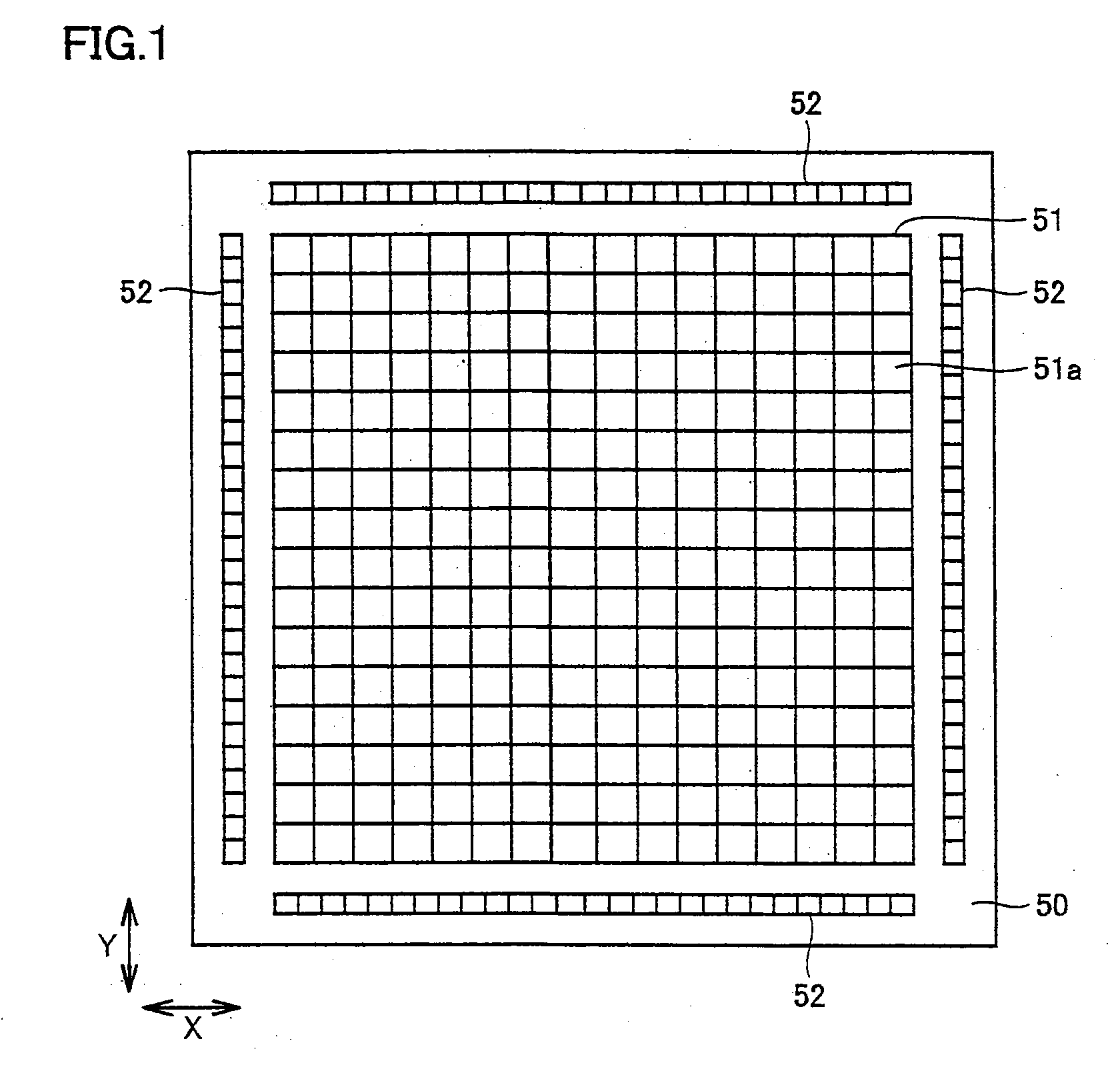
[0070]With reference to FIG. 1, a semiconductor device (e.g., a semiconductor chip) 50 has a surface mainly having a standard cell region 51, an input / output (I / O) cell region 52 surrounding standard cell region 51, and a pad (not shown) used for inputting / outputting externally.

[0071]In the figure, standard cell region 51 has a plurality of standard cells 51 as arranged in a matrix (or rows and columns) extending in a direction X and a direction Y orthogonal to direction X. The plurality of standard cells 51as are each surrounded by peripheral edges extending in direction X and opposite to each other, and peripheral edges extending in direction Y and opposite to each other. A standard cell is a cell for a logic element. It is arranged by automatic placement to configure a desired function in a semiconductor device. For an SOC using a standard cell library, standard cell region 51 has formed therein a central processing unit (CPU), a random access memory (RAM), a first-in first-out (...

second embodiment

[0096]With reference to FIG. 9, while the first embodiment provides power supply wiring VD and grounding wiring VS, the present embodiment instead provides a power supply wiring VDw and a grounding wiring VSw. Power supply wiring VDw and grounding wiring VS each have a width Ww. Width Ww is larger than a width Ws of each of pMIS wiring M1p and nMIS wiring M1n.

[0097]The remainder in configuration is substantially identical to that described above in the first embodiment. Accordingly, identical or corresponding elements are identically denoted and will not be described repeatedly.

[0098]In accordance with the present embodiment, power supply wiring VDw and grounding wiring VSw each increased in width Ww can have a reduced voltage drop while pMIS wiring M1p and nMIS wiring M1n, which significantly affect the size of standard cell Cff, can be reduced in width Ws. This can reduce power supply voltage drop, which is disadvantageous for a fast operation in particular, and also reduce stand...

third embodiment

[0099]With reference to FIG. 10, the present embodiment provides a semiconductor device having standard cells Civ, Cnd, Cnr, and Cfl. Standard cells Civ, Cnd, Cnr, Cfl are divided into a plurality of rows and thus arranged, and are arranged in each row in direction X as shown in the figure.

[0100]Standard cells Civ, Cnd, and Cnr are provided to implement the functions of an inverter, a 2NAND, and a 2NOR, respectively. The 2NAND is an NAND having two input systems, and the 2NOR is an NOR having two input systems. Furthermore, standard cell Cfl is a filler cell.

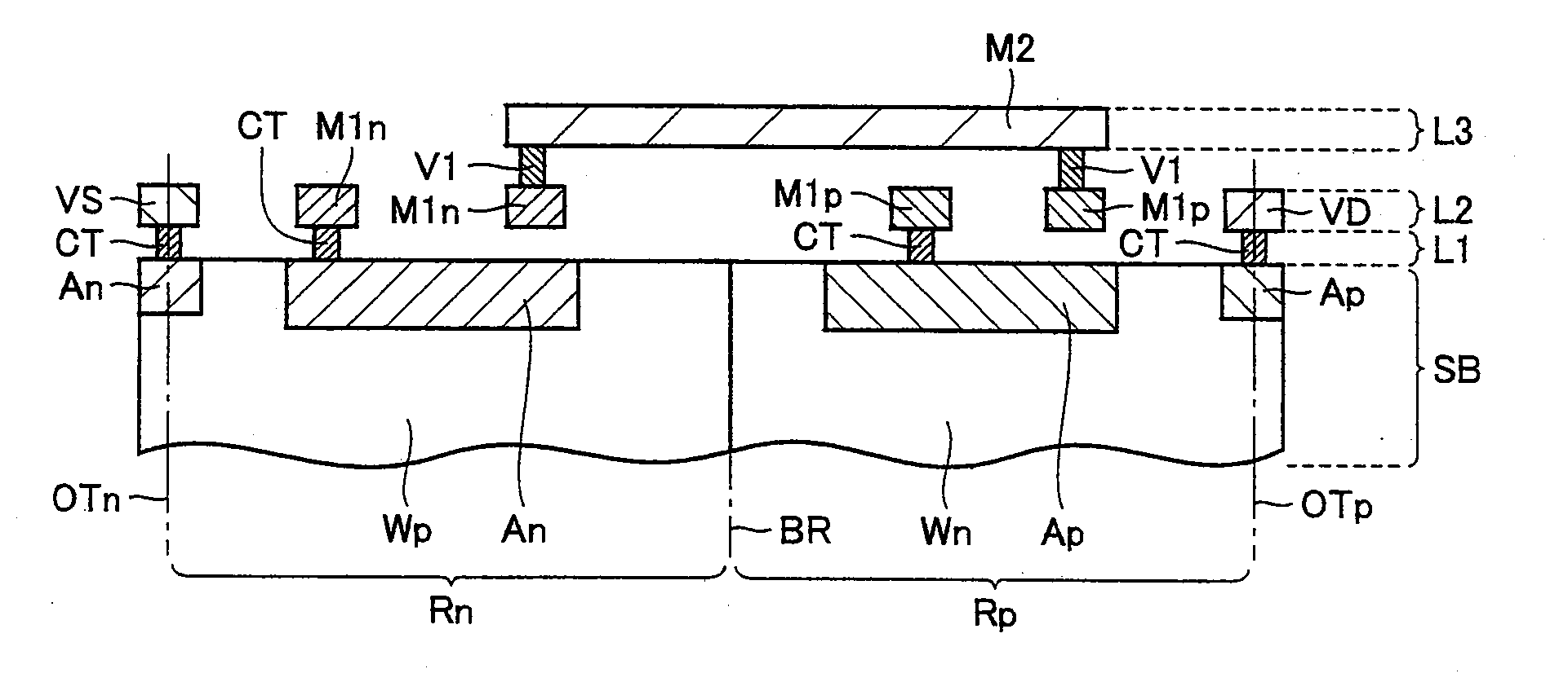
[0101]With reference to FIGS. 11-14, the present embodiment provides a semiconductor device having standard cells Civ, Cnd, Cnr each similar in configuration to standard cell Cff of the first embodiment. More specifically, the present embodiment provides a semiconductor device having standard cells Civ, Cnd, Cnr each having a semiconductor substrate and first to third layers. The semiconductor substrate has pMIS region Rp and nM...


PUM


Abstract

A pMIS region is provided between a boundary extending in a first direction and passing through each of a plurality of standard cells and a first peripheral edge. An nMIS region is provided between the boundary and a second peripheral edge. A power supply wiring and a grounding wiring extend along the first and second peripheral edges, respectively. A plurality of pMIS wirings and a plurality of nMIS wirings are arranged on a plurality of first virtual lines and a plurality of second virtual lines, respectively, extending in the first direction and arranged with a single pitch in a second direction. The first virtual line that is the closest to the boundary and the second virtual line that is the closest to the boundary have therebetween a spacing larger than the single pitch.

Description

BACKGROUND OF THE INVENTION[0001]1. Field of the Invention[0002]The present invention relates generally to semiconductor devices and particularly to semiconductor devices having arranged multiple standard cells.[0003]2. Description of the Background Art[0004]For designing semiconductor devices, in the 45 nm generation in particular, there has been adopted or considered a technique for designing referred to as a restrictive design rule (RDR). More specifically, the RDR is a design rule with severe constraints. It does not employ a two dimensional layout having a metal wiring and a poly wiring each bent. Rather, it employs a one dimensional layout prohibiting such bending. This reduces or eliminates variation attributed to dependency on geometry of transistors, wirings and the like, and furthermore, reduces or eliminates design rule check (DRC), optical proximity correction (OPC), lithography verification and other similar electronics design automation (EDA) loads. The RDR can thus re...

Claims


Application Information

Patent Timeline
Patent Type & Authority Applications(United States)
IPC IPC(8): H01L27/088
CPCH01L27/0207H01L27/092H01L27/0928H01L27/11898H01L27/11803
Inventor TSUDA, NOBUHIRONISHIMAKI, HIDEKATSUOMURA, HIROSHIYOSHIFUKU, YUKO
Owner RENESAS ELECTRONICS CORP
Why Eureka
Try Eureka