Semiconductor device, method for mounting semiconductor device, and mounting structure of semiconductor device
a semiconductor device and mounting method technology, applied in the direction of printed circuit, sustainable manufacturing/processing, final product manufacturing, etc., can solve the problems of increasing the size of the package, increasing the inductance, and difficult to increase the processing speed of the semiconductor device, so as to achieve easy mounting and high mounting reliability
- Summary
- Abstract
- Description
- Claims
- Application Information
AI Technical Summary
Benefits of technology
Problems solved by technology
Method used
Image

Examples
first embodiment
[0036]The following describes one embodiment of the present invention with reference to FIG. 1 through FIG. 6.
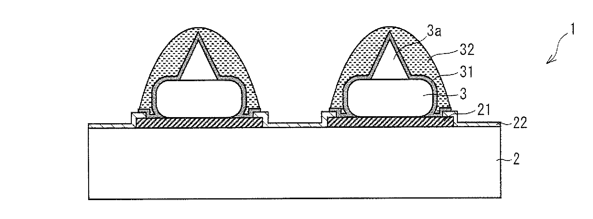
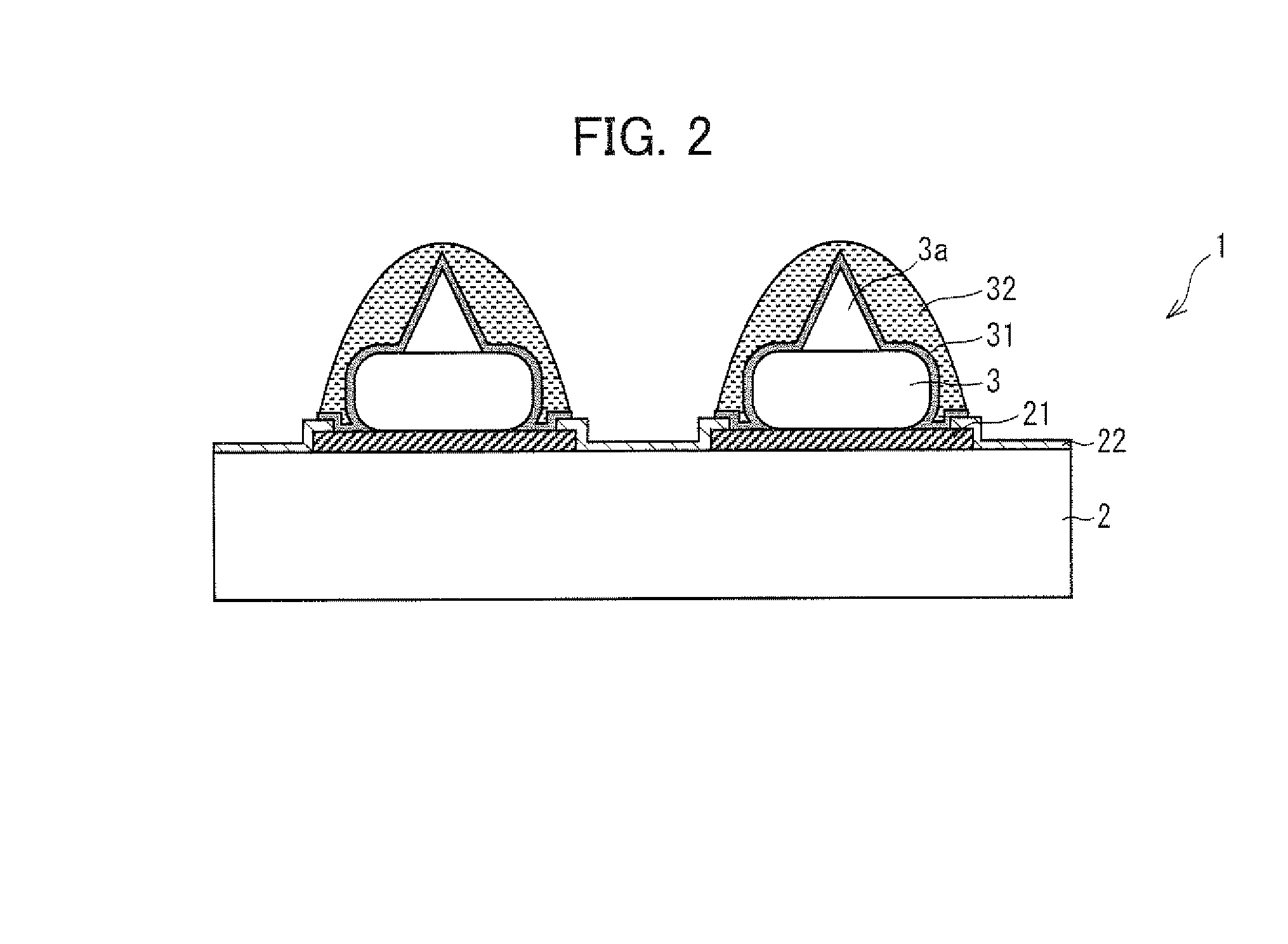
[0037]FIG. 2 is a cross-section view illustrating a semiconductor device 1 according to the present embodiment. The semiconductor device 1 includes a semiconductor substrate 2 and an Au bump (metal bump) 3. The surface of the semiconductor substrate 2 is provided with an electrode 21 and a surface protection film 22. The Au bump 3 is provided on the electrode 21 and has a projection (protruded portion) 3a having a cone-shape. This allows the projection 3a to penetrate through a surface oxide layer of solder with a small weight during flip-chip bonding.
[0038]The Au bump 3 has a Ni layer 31 on its surface, and the Ni layer 31 has solder (solder layer) 32 thereon. The Ni layer 31 protects the Au bump 3 from dissolution. Also, the Ni layer 31 protects the projection 3a so that the projection 3a does not dissolve in the solder 32 during flip-chip bonding. This increases a connect...
second embodiment
[0053]Another embodiment of the present invention is described below with reference to FIG. 7 through FIG. 11.
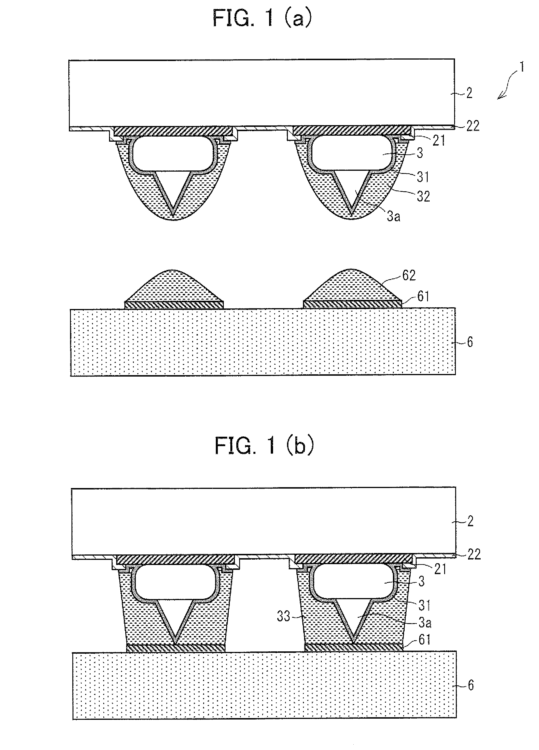
[0054]FIG. 7 is a cross-section view illustrating an arrangement of a semiconductor device 11 according to the present embodiment. In the semiconductor device 1 illustrated in FIG. 1, the solder 32 is supplied on the whole surface of the Au bump 3. Instead of this arrangement of the semiconductor device 1, the semiconductor device 11 has such an arrangement that solder (solder layer) 34 is supplied only on a part of a Ni layer 31, the part covering: a projection 3a of an Au bump 3; and the top surface of the Au bump 3 having a pedestal-shape. Compared with the arrangement of the semiconductor device 1 illustrated in FIG. 1, this arrangement of the semiconductor device 11 ensures a less amount of solder. On the other hand, the arrangement of the semiconductor device 11 can reduce the possibility of a short circuit between bumps during supply of solder or during flip-chip bond...
PUM
 Abstract
Description
Claims
Application Information
 - R&D Engineer
- R&D Manager
- IP Professional
- Industry Leading Data Capabilities
- Powerful AI technology
- Patent DNA Extraction
Browse by: Latest US Patents, China's latest patents, Technical Efficacy Thesaurus, Application Domain, Technology Topic.
© 2024 PatSnap. All rights reserved.Legal|Privacy policy|Modern Slavery Act Transparency Statement|Sitemap