Wafer level chip size package having redistribution layers

a technology of redistribution layer and chip size, applied in the direction of electrical apparatus, semiconductor device details, semiconductor/solid-state device devices, etc., can solve the problems of increasing manufacturing costs and complicated packaging

Active Publication Date: 2011-07-12
AMKOR TECH SINGAPORE HLDG PTE LTD
View PDF13 Cites 111 Cited by
  • Summary
  • Abstract
  • Description
  • Claims
  • Application Information

AI Technical Summary

Problems solved by technology

Therefore, since the number of passivation layers is to be increased...

Method used


Image

  • Wafer level chip size package having redistribution layers
  • Wafer level chip size package having redistribution layers
  • Wafer level chip size package having redistribution layers

Examples


Embodiment Construction

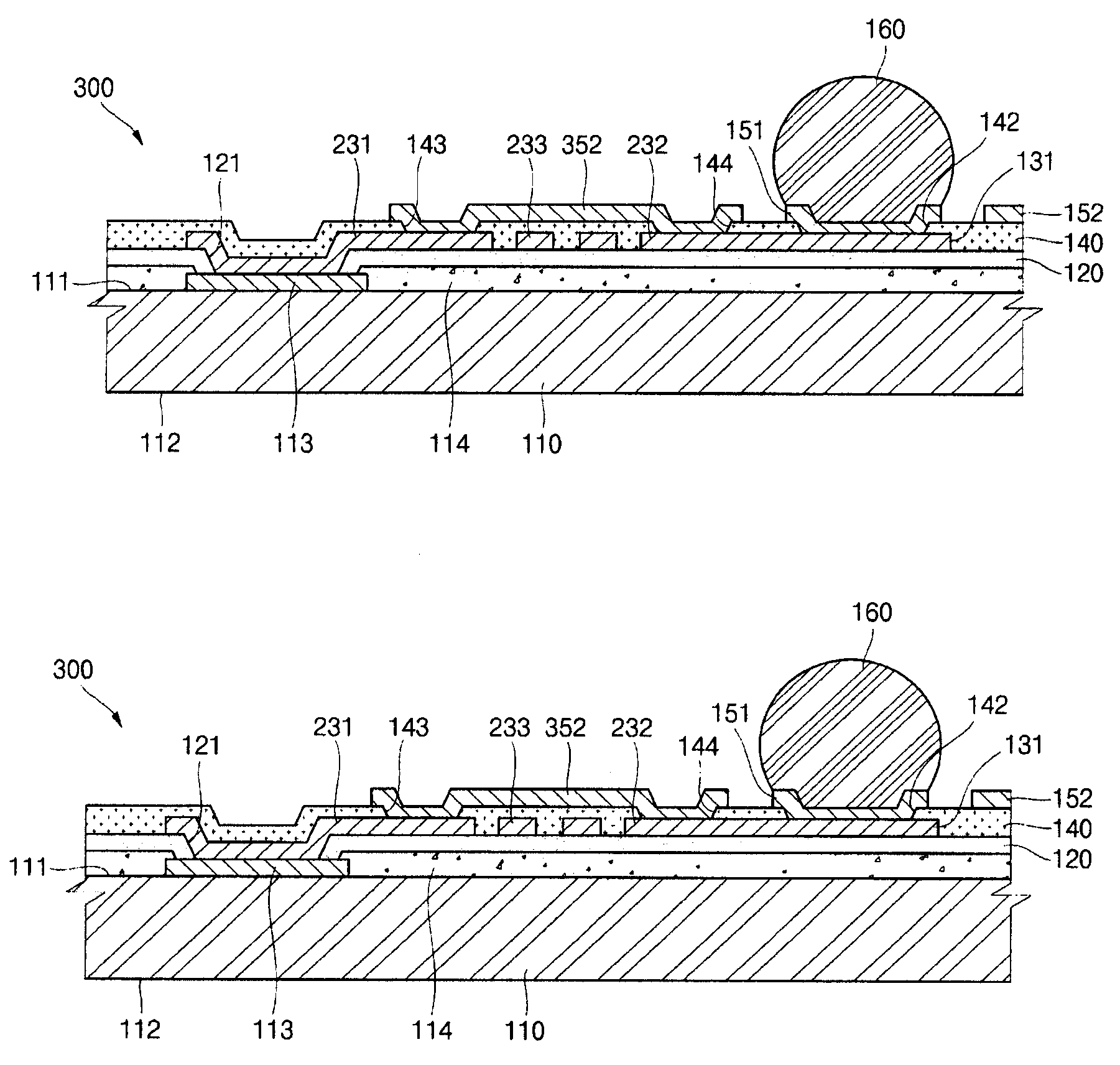
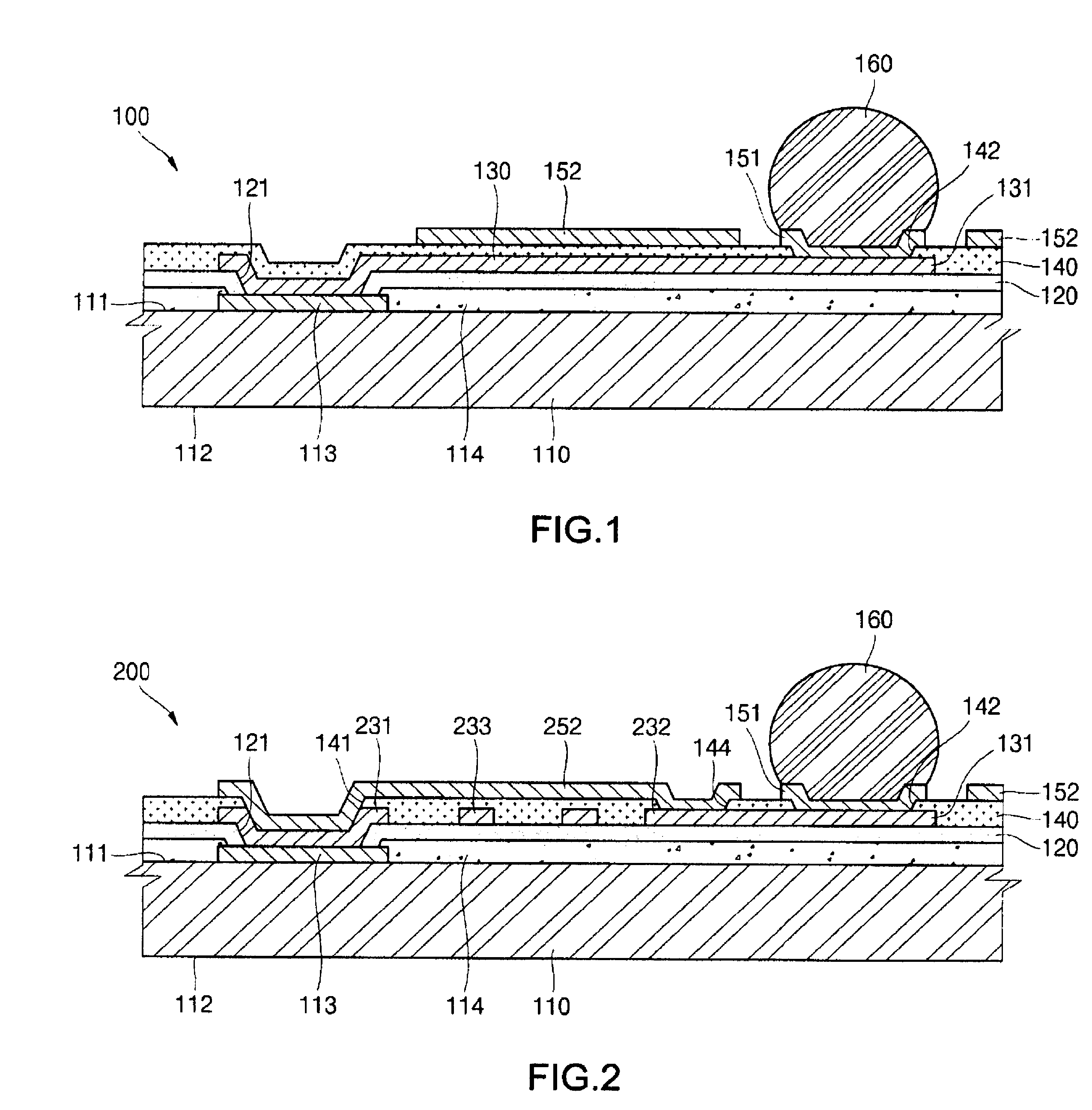
[0021]Referring to FIG. 1, a sectional view of a wafer level chip size package (WLCSP) 100 according to an embodiment of the present invention is illustrated.

[0022]As illustrated in FIG. 1, the WLCSP 100 according to the embodiment of the present invention includes a semiconductor die 110, a first dielectric layer 120, a redistribution layer 130, a second dielectric layer 140, a first under bump metallurgy (UBM) layer 151, a second UBM layer 152, and a solder ball 160.

[0023]The semiconductor die 110 includes a first approximately planar surface 111 and a second approximately planar surface 112 as the opposite surface of the first surface 111. The semiconductor die 110 includes at least one bond pad 113, which can be formed on the first surface 111. Furthermore, a passivation layer 114 can be formed on the first surface 111 that is the outer circumference of the bond pad 113. The passivation layer 114 can be made of one selected from the group of PolyImide (PI), Benzo Cyclo Butene (B...


PUM


Abstract

A wafer level chip size package (WLCSP) and a method of manufacturing the same are disclosed. Lands are formed at the ends of redistribution layers. The redistribution layers excluding the lands and a first dielectric layer are covered with a second dielectric layer. After forming a first under bump metallurgy (UBM) layer on the land, a solder ball is reflowed to the first UBM layer. A second UBM layer is widely formed on the entire second dielectric layer that is the outer circumference of the first UBM layer and is connected to the redistribution layer through a via-hole. Therefore, the second UBM layer having a large area can be used as a ground plane or a power plane. In addition, the second UBM layer can electrically connect the redistribution layers physically separated from each other. Therefore, the plurality of redistribution layers can cross each other without being electrically shorted with each other.

Description

BACKGROUND OF THE INVENTION[0001]1. Field of the Invention[0002]The present invention relates to a wafer level chip size package (WLCSP) and a method of manufacturing the same.[0003]2. Description of the Related Art[0004]A desire to make electronic products small, light, and have high performance develops into a desire to make electronic parts small, light, and have high performance. Such a desire causes development in various packaging technologies with development in technologies of designing and manufacturing semiconductors. The representative examples of the packaging technologies are ball grid array (BGA), flip-chip, and chip size package (CSP) based on area array and a surface-mount packaging. Among the above, the CSP is a packaging technology spotlighted by enabling a small package having a size the same as a real chip size to be developed. In particular, in a wafer level chip size package (WLCSP), the packaging is performed in a wafer level so that packaging costs per a chip...

Claims


Application Information

Patent Timeline
IPC IPC(8): H01L23/48
CPCH01L24/11H01L23/552H01L2224/13111H01L24/13H01L2224/0231H01L2224/13021H01L2224/13099H01L2924/01022H01L2924/01029H01L2924/0103H01L2924/01047H01L2924/01078H01L2924/01079H01L2924/01082H01L2924/3025H01L2224/0558H01L2224/05644H01L2924/01033H01L2924/01074H01L2924/01075H01L2924/014H01L2924/0001H01L2224/0401H01L2224/0233H01L2924/00014H01L2924/01083H01L2224/0235H01L2224/02351H01L2224/05008H01L2224/05569H01L2224/05572H01L2224/11334
Inventor PARK, NO SUNCHUNG, YOUNG SUKSHIM, JAE BEOM
Owner AMKOR TECH SINGAPORE HLDG PTE LTD
Why Eureka
Try Eureka