Dual interface inlays

a dual-interface, inlay technology, applied in the direction of instruments, burglar alarm mechanical actuation, protective material radiating elements, etc., can solve the problems of difficult to guarantee the life time of the finished product with certainty, operational failure, and local heating of the wire conductor, so as to achieve the effect of increasing the surface area

Inactive Publication Date: 2011-07-19
HID GLOBAL GMBH +1
View PDF100 Cites 45 Cited by
  • Summary
  • Abstract
  • Description
  • Claims
  • Application Information

AI Technical Summary

Problems solved by technology

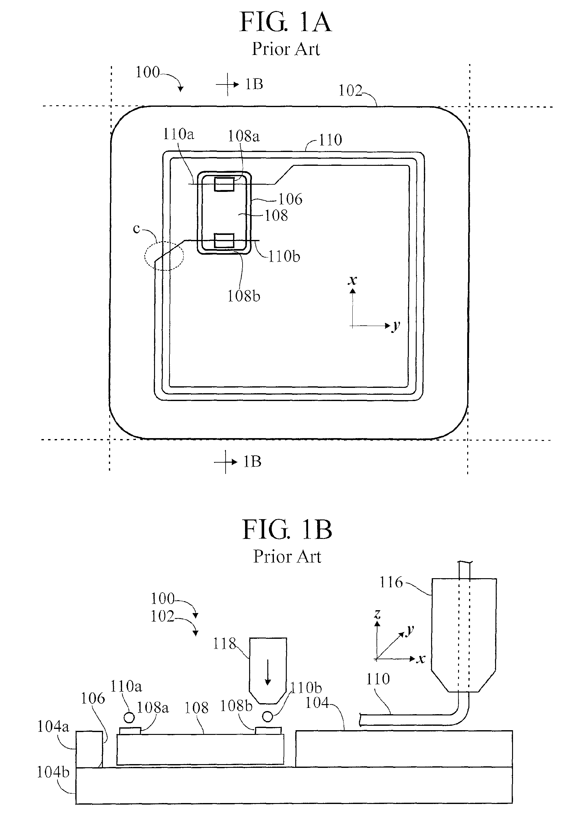
The wire conductor is fed through the wire guide tool, emerges from the tip, and by application of pressure and ultrasonic energy the wire conductor is “rubbed” into the substrate, resulting in localized heating of the wire conductor and subsequent sinking of the wire conductor into the substrate material during the movement of the wire guide tool.
Apart from yield loss during production, the life time of the finished product is difficult to guarantee with certainty, as torsion and bending of the card body at the position of the chip module results in operational failure.
Although the problem of a weak interconnection of the antenna to the contact chip module is partially resolved, there are serious problems of chip breakage during both (pre & final) lamination processes as well as the shrinkage of the materials leaving a spoiled printed sheet around the contact chip module area.
To compensate for shrinkage, it is possible to match the grain direction of the materials to one another and to provide for indents in the lamination plates, but the overall yield loss is significant.
Low power levels can lead to incomplete wetting and the formation of voids, both of which can weaken the joint.

Method used


Image

  • Dual interface inlays
  • Dual interface inlays
  • Dual interface inlays

Examples


Embodiment Construction

[0075]In the following description, various aspects of techniques for making dual interface cards will be described. For the purpose of explanation, specific configurations and details are set forth in order to provide a thorough understanding of the techniques. However, it will also be apparent to one skilled in the art that the techniques may be practiced without specific details being presented herein. Furthermore, well-known features may be omitted or simplified in order not to obscure the description(s) of the techniques.

[0076]Various “embodiments” of the invention will be discussed. An embodiment is an example or implementation of one or more aspects of the invention(s). Although various features of the invention may be described in the context of a single embodiment, the features may also be provided separately or in any suitable combination with one another.

[0077]It should be understood that the phraseology and terminology employed herein is not to be construed as limiting, ...


PUM

PropertyMeasurementUnit
diameteraaaaaaaaaa
diameteraaaaaaaaaa
diameteraaaaaaaaaa

Abstract

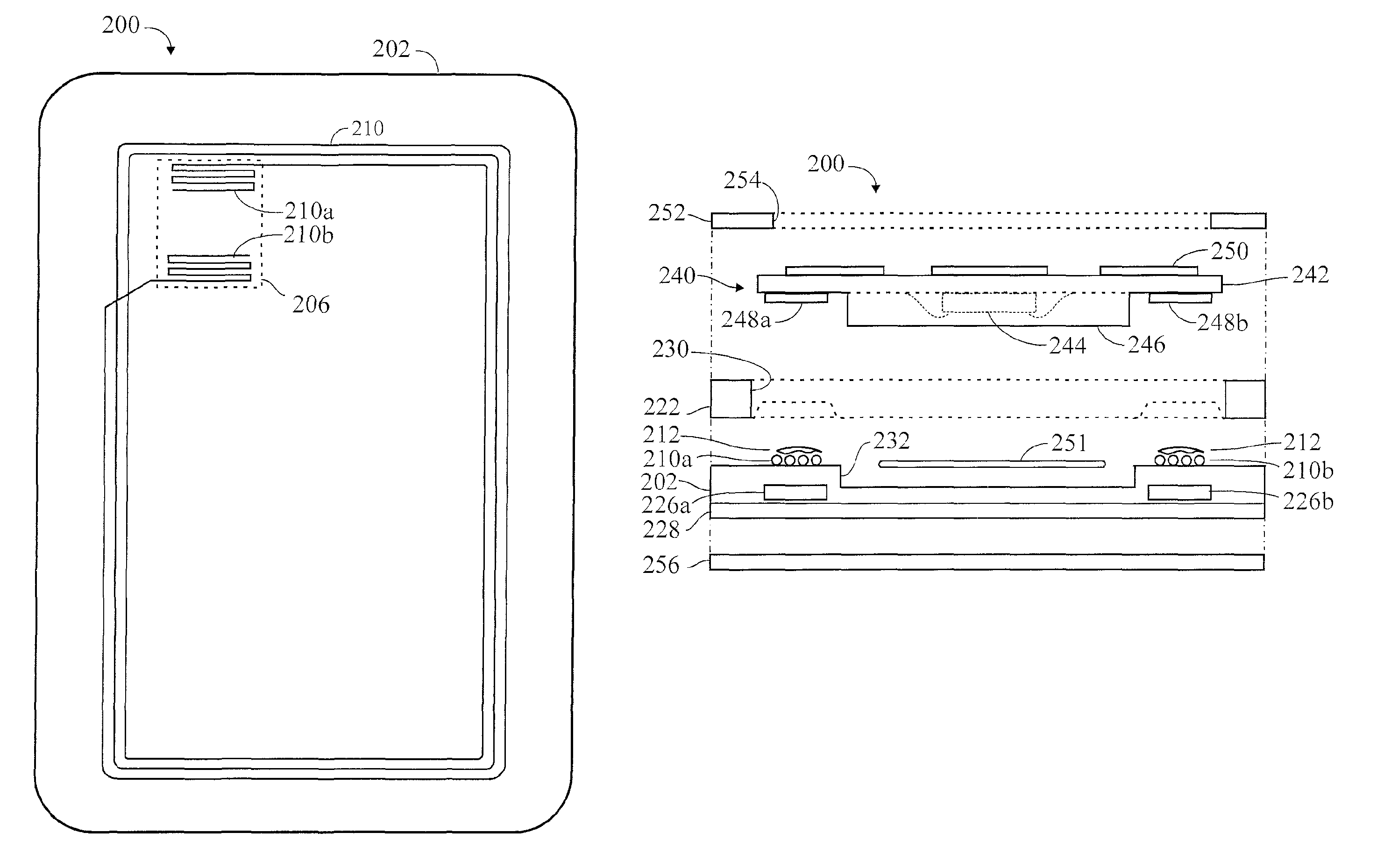
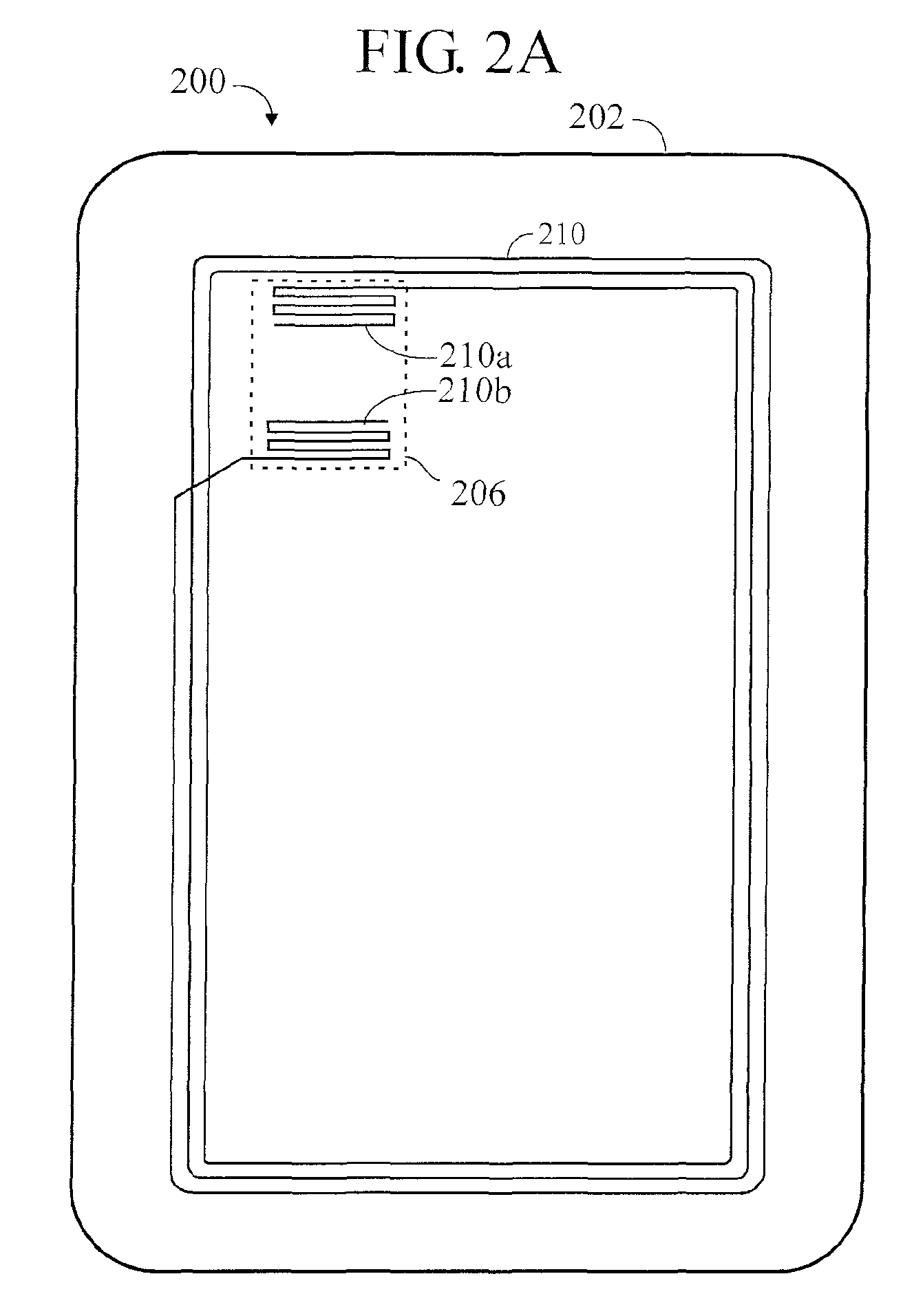
A dual interface inlay having a bottom sheet; an antenna wire mounted to the top surface of the bottom sheet; end portions of the antenna wire formed with squiggles or meanders forming contact areas of increased surface area for subsequent attachment of a chip or chip module to the antenna wire; conductive material applied to the end portions of the antenna wire; a top sheet disposed over the bottom sheet for lamination thereto; and recesses formed in a bottom surface of the top sheet, at positions corresponding to the contact area. The antenna wire may be insulated wire, and insulation may be removed from the end portions of the antenna wire. Silicon cushions may be disposed in the bottom sheet under the contact areas.

Description

CROSS-REFERENCE TO RELATED APPLICATIONS[0001]This patent application claims benefit of U.S. Provisional Application No. 60 / 938,454 filed 17 May 2007 by Finn (“S11ppa”).FIELD OF THE INVENTION[0002]The invention relates primarily to techniques for fabricating dual interface cards comprising an antenna embedded in one substrate, and laminated with upper and lower substrates whereby a chip module is connected to the antenna prior or after final lamination.BACKGROUND OF THE INVENTION[0003]A conventional method to produce an inlay site containing a high frequency RFID chip and an antenna embedded into a multi-layer substrate and connected to the terminals (terminal areas) of the RFID chip is to first position the RFID chip in a recess, supported by a lower substrate layer, then start embedding (countersinking) a wire conductor onto or into the top substrate layer in the direction of the RFID chip, then guiding the wire conductor over a first terminal area of the RFID chip, then continue t...

Claims


Application Information

Patent Timeline
Patent Type & Authority Patents(United States)
IPC IPC(8): G06K19/06H01Q1/40H01Q1/36G08B13/14
CPCG06K19/077G06K19/0775G06K19/07769Y10T29/49124Y10T29/49016H01L2224/16225H01L2224/48091H01L2224/48227H01L2924/00014
Inventor FINN, DAVID
Owner HID GLOBAL GMBH
Why Eureka
Try Eureka