Semiconductor test device with heating circuit

a technology of heating circuit and semiconductor circuit, which is applied in the direction of measurement devices, electrical testing, instruments, etc., can solve the problems that the conventional thermal fatigue testing of a semiconductor circuit may become excessively time-consuming, and the reliability of the semiconductor,

Inactive Publication Date: 2006-03-30
AGERE SYST INC
View PDF39 Cites 21 Cited by
  • Summary
  • Abstract
  • Description
  • Claims
  • Application Information

AI Technical Summary

Problems solved by technology

A well-known problem area affecting semiconductor reliability is thermal reliability.
However, conventional thermal fatigue testing of a semiconductor circuit may become excessively time consuming due to the amount of

Method used


Image

  • Semiconductor test device with heating circuit
  • Semiconductor test device with heating circuit
  • Semiconductor test device with heating circuit

Examples


Embodiment Construction

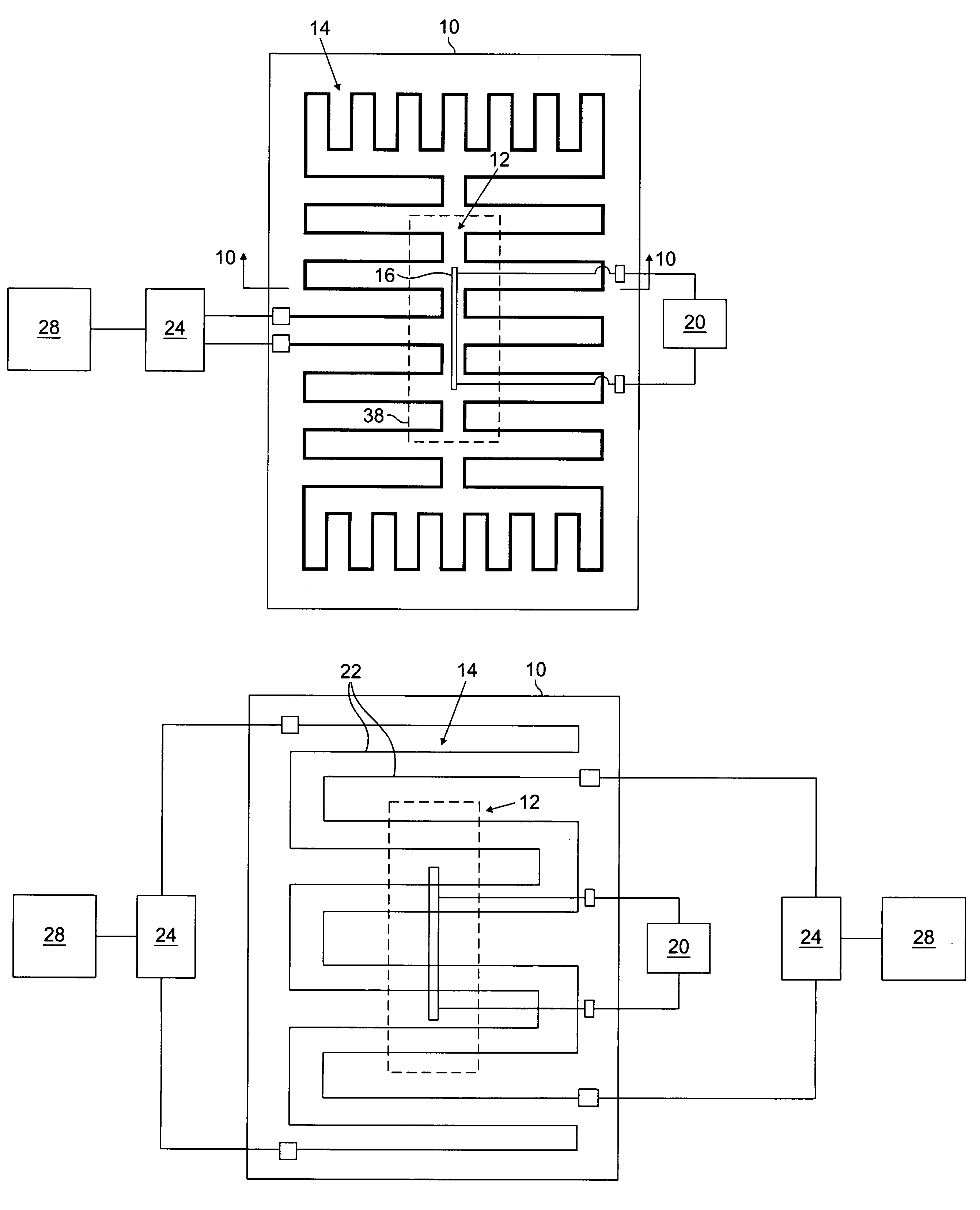
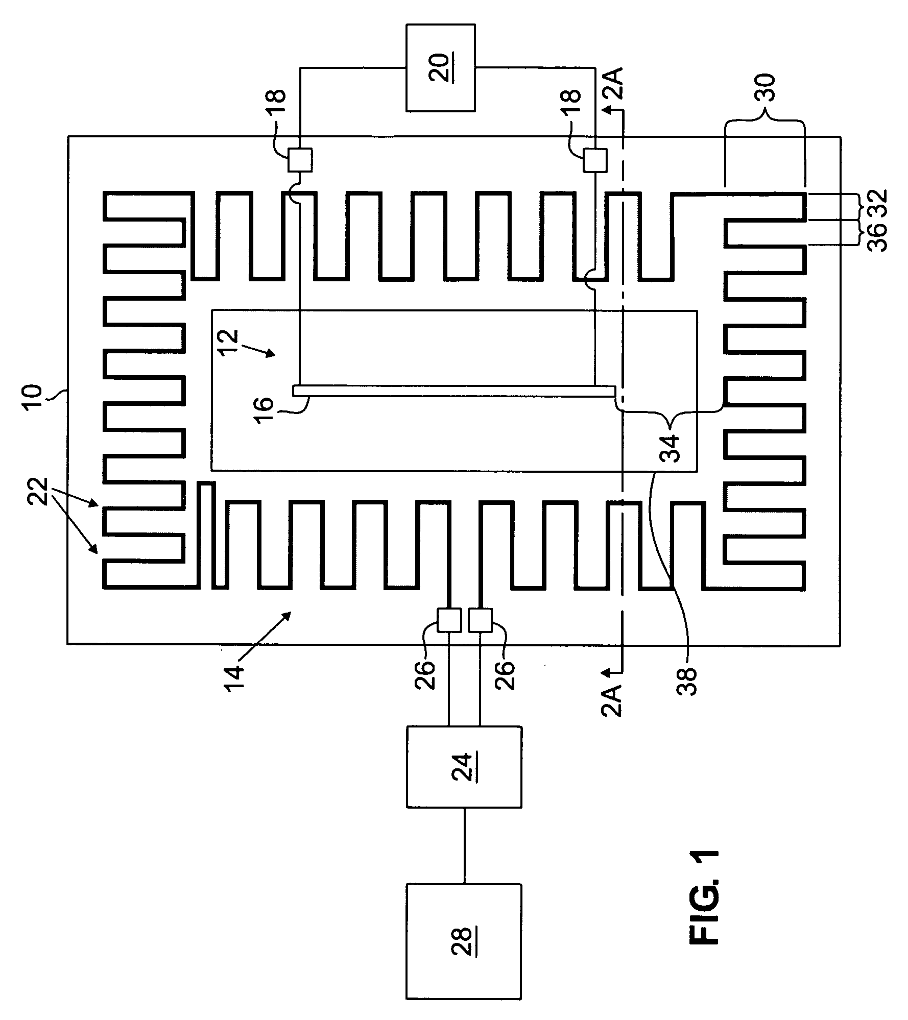
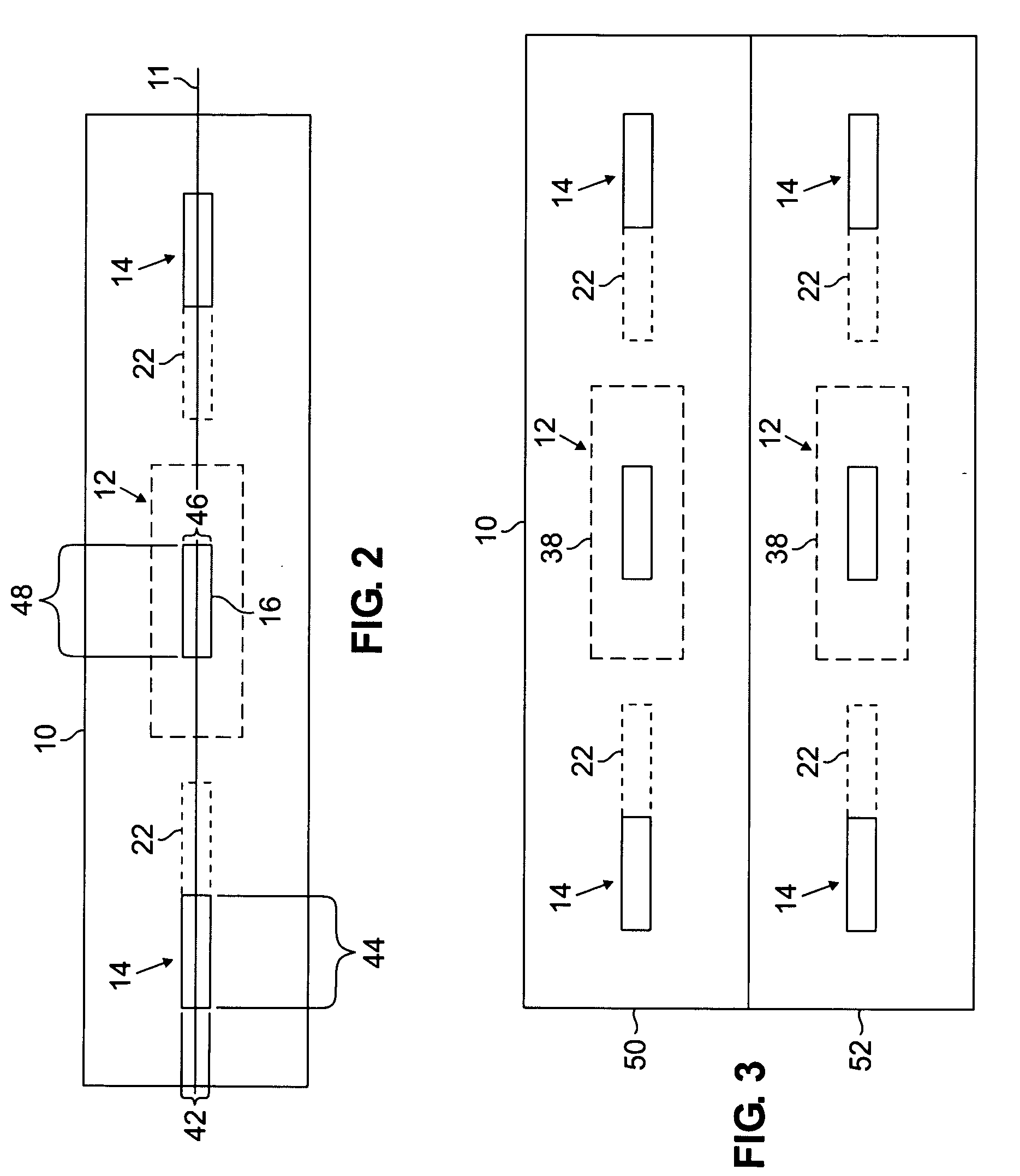
[0018]FIG. 1 shows a top view of an exemplary semiconductor test wafer 10 cut away to reveal a reliability test circuit 12 and an innovative heating circuit 14 integrally formed with the wafer 10 adjacent the reliability test circuit 12. In an aspect of the invention, the reliability test circuit 12 may include a known standard Joint Electron Device Engineering Council (JEDEC) tester, as described in JEDEC standard JESD87, or an extrusion test circuit used to measure metal extrusion phenomena during electro-migration testing, or a similar test structure used to assess interconnect reliability for resistance to electro-migration, stress-induced voiding, or stress migration. In an aspect of the invention, the reliability test circuit 12 may include one or more conductor traces 16 having contacts 18 for applying and measuring electrical signals by a tester 20 connected to the contacts 18. Typically, the conductor trace 16 is disposed coplanar with a horizontal plane of the test circuit...


PUM


Abstract

A semiconductor test device includes a test circuit having contacts for applying an electrical signal and measuring electrical parameters of the test circuit. The semiconductor test device also includes an integrally formed heating circuit comprising at least one circuit meander positioned adjacent the test circuit for raising a temperature within a portion of the test circuit.

Description

FIELD OF THE INVENTION [0001] The invention is generally related to the field of semiconductor devices and, more particularly, to a semiconductor wafer having an integrally formed heating element. BACKGROUND OF THE INVENTION [0002] A well-known problem area affecting semiconductor reliability is thermal reliability. Consequently, thermal analysis is an important part of testing semiconductor devices. In particular, measurements of cyclic thermal loading on interconnect behavior, such as thermal fatigue and Joule heating that affect the known phenomena of electro-migration and stress migration of interconnects, are necessary to assess reliability of a semiconductor circuit. Conventional techniques for assessing the reliability of a semiconductor circuit include assembling the circuit in a ceramic or similar package, heating the package using external heating sources such as by placing the package in a temperature controlled chamber, applying heat to the package, while applying a dire...

Claims


Application Information

Patent Timeline
IPC IPC(8): G01R31/02
CPCG01R31/2877G01R31/2856
Inventor KANG, SEUNG H.KARTHIKEYAN, SUBRAMANIANMERCHANT, SAILESHMULLIN, LISA E.
Owner AGERE SYST INC
Why Eureka
Try Eureka